Semiconductor device and method of manufacturing semiconductor device

Active Publication Date: 2017-03-16
FUJI ELECTRIC CO LTD
View PDF7 Cites 4 Cited by
  • Summary
  • Abstract
  • Description
  • Claims
  • Application Information

AI Technical Summary

Benefits of technology

[0044]In the invention described above, during normal operation the voltage (a second voltage) applied to a device to be protected can be clamped to a voltage equal to the sum of the reverse voltage (breakdown voltage) of the first diode and the forward voltage of the second diode, thereby making it possible to prevent a high voltage from being applied to the device to be protected. Furthermore, the second diode that is made from the polycrystalline silicon layer does not get biased in the reverse direction (in which the variation in voltage can be significant), thereby making it possible to reduce variations in the voltage applied to the device to be protected. In addition, during abnormal operation, any forward current flowing through the first diode is blocked by the second diode,

Problems solved by technology

The currents 151 and 152 are unintended currents that were not accounted for in the design of the circuit (the powe

Method used


Image

  • Semiconductor device and method of manufacturing semiconductor device
  • Semiconductor device and method of manufacturing semiconductor device
  • Semiconductor device and method of manufacturing semiconductor device

Examples


Example

Embodiment 1

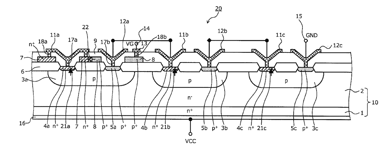
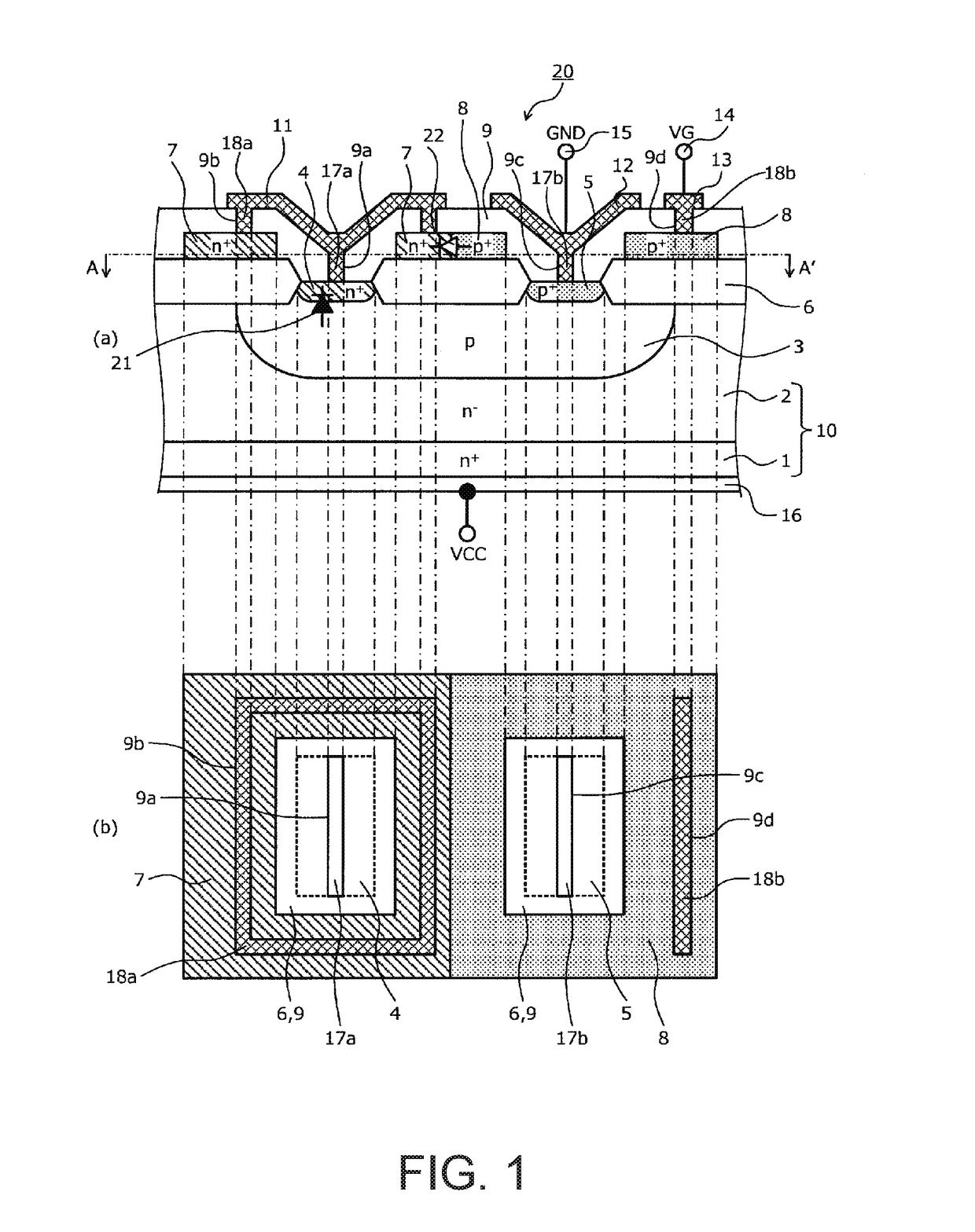
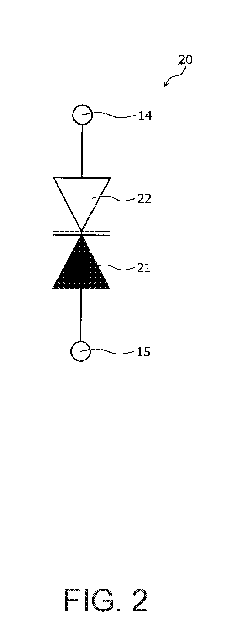
[0064]A semiconductor device according to Embodiment 1 includes an n-channel MOSFET and a lateral protection device for protecting (providing gate protection for) a gate insulating film of the n-channel MOSFET, and the n-channel MOSFET and the lateral protection device are both formed on the same semiconductor substrate (semiconductor chip). FIG. 1 illustrates the main components of the structure of the semiconductor device according to Embodiment 1. FIG. 1 only depicts a lateral protection device 20 of the semiconductor device according to Embodiment 1, and other components that are formed in the same semiconductor substrate as the lateral protection device 20 are not illustrated in the figure. FIG. 1(a) illustrates the cross-sectional structure of the lateral protection device 20, and FIG. 1(b) is a plan view of a section taken along line A-A′ in FIG. 1(a). FIG. 2 is a circuit diagram illustrating an equivalent circuit for the configuration illustrated in FIG. 1.

[0065]...

Example

Embodiment 2

[0093]Next, the structure of a semiconductor device according to Embodiment 2 will be described. FIG. 7 illustrates the main components of the structure of the semiconductor device according to Embodiment 2. FIG. 7 only depicts a lateral protection device 80 of the semiconductor device according to Embodiment 2, and other components are not illustrated in the figure. The planar layout of the lateral protection device 80 as taken along line B-B′ in FIG. 7 is the same as the planar layout of the lateral protection device according to Embodiment 1 (see FIG. 1(b)) except in that the conductivity type (p-type or n-type) of each region is inverted. FIG. 8 is a circuit diagram illustrating an equivalent circuit for the configuration illustrated in FIG. 7. The semiconductor device according to Embodiment 2 is different than the semiconductor device according to Embodiment 1 in that the conductivity types (p-type or n-type) of the semiconductor substrate, the semiconductor region...

Example

Embodiment 3

[0108]A semiconductor device according to Embodiment 3 includes the lateral protection device 30 of Embodiment 1 (see FIG. 6B) as well as other components that are arranged on the same semiconductor substrate 10. FIG. 10 illustrates the structure of the semiconductor device according to Embodiment 3. FIG. 10 illustrates an example of a high-side power IC for use in a vehicle that includes an output stage vertical MOSFET 210, a lateral CMOS which is a circuit device for a control circuit for the vertical MOSFET 210, and the lateral protection device 30, which are all arranged on the same semiconductor substrate 10. The power IC also includes a lateral p-channel MOSFET and a lateral n-channel MOSFET connected together complementarily to form the lateral CMOS. However, FIG. 10 only depicts the lateral n-channel MOSFET 220. The lateral protection device 30 protects a gate electrode 225 of the lateral n-channel MOSFET 220.

[0109]More specifically, the semiconductor substrate 1...


PUM


Abstract

A diffusion diode including a p+ diffusion region, a p-type diffusion region, and an n+ diffusion region is formed in the front surface of a semiconductor substrate. A polysilicon diode including a p+ layer and an n+ layer is formed on top of a local insulating film formed on the front surface of the semiconductor substrate and faces the diffusion diode in the depth direction. The diffusion diode and the polysilicon diode are reverse-connected by electrically connecting the n+ diffusion region to the n+ layer, thereby forming a lateral protection device. The p+ layer and p+ diffusion region are respectively electrically connected to a high voltage first terminal and a low voltage second terminal of the lateral protection device. The polysilicon diode blocks a forward current generated in the diffusion diode when the electric potential of the first terminal becomes lower than the electric potential of the second terminal.

Description

BACKGROUND OF THE INVENTION[0001]Technical Field[0002]The present invention relates to a semiconductor device and a method of manufacturing the semiconductor device.[0003]Background Art[0004]Power integrated circuits (power ICs) that include both a vertical power semiconductor device and a lateral power semiconductor device for controlling / providing a protection circuit for the vertical power semiconductor device are a well-known conventional technology for increasing the reliability and reducing the size and cost of power semiconductor devices (see Patent Documents 1 and 2, for example). One example of such a conventional power semiconductor device is a power IC that includes an output stage vertical power semiconductor device, a circuit device for a control circuit, and a protection device that are all mounted on the same semiconductor substrate. FIG. 11 is a cross-sectional view illustrating the structure of an example of such a conventional semiconductor device.[0005]The convent...

Claims


Application Information

Patent Timeline
IPC IPC(8): H01L27/02H01L29/78H01L29/866H01L29/66H01L29/04H01L29/16
CPCH01L2224/48137H01L29/0696H01L29/7813H01L27/0629H01L29/7395H01L29/7808H01L29/04H01L29/16H01L29/866H01L29/66106H01L27/0255H01L29/0649H01L27/0814H03K17/08122H03K17/08142H03K17/0822
Inventor TOYODA, YOSHIAKI
Owner FUJI ELECTRIC CO LTD
Why Eureka
Try Eureka