
Semiconductor device and method of producing the same

Inactive Publication Date: 2017-04-27
SUMITOMO ELECTRIC IND LTD
View PDF6 Cites 15 Cited by
  • Summary
  • Abstract
  • Description
  • Claims
  • Application Information

AI Technical Summary

Benefits of technology

This patent describes a process and device type for making and using a semiconductor called a high electron-mobility transistor (HEMT). The process includes steps of growing a semiconductor stack, implanting impurities, forming an insulating film, annealing the semiconductor stack, removing the insulating film, and finally forming a gate electrode. The device type includes a semiconductor stack with n+ regions, an insulating film with an opening, and source and drain electrodes on the surface of the n+ regions. The surface of the semiconductor stack in the space is lower than the surface of the n+ regions. The technical effect of this patent is to provide a process and device type for making and using a nitride semiconductor HEMT with improved performance and reliability.

Problems solved by technology

However, such annealing sometimes degrades the quality of the mother semiconductor materials to be processed; in particular, a surface of the semiconductor material is possibly damaged during the annealing.
Such a surface region degraded in the stoichiometry thereof may increase leak currents between the electrodes and degrade the long-term reliability of the device.
However, even such an inorganic film covers the surface; the inorganic film may not thoroughly protect the nitrogen (N) from sublimating from the surface.
A silicon oxide (SiOx) is known as a material substitutable for SiN; but SiON easily causes oxidization of the surface.

Method used


Image

  • Semiconductor device and method of producing the same
  • Semiconductor device and method of producing the same
  • Semiconductor device and method of producing the same

Examples


Embodiment Construction

[0019]Next, embodiment of a semiconductor device according to the present invention will be described as referring to accompanying drawings. In the description of the drawings, numerals or symbols same with or similar to each other will refer to elements same with or similar to each other without duplicating explanations.

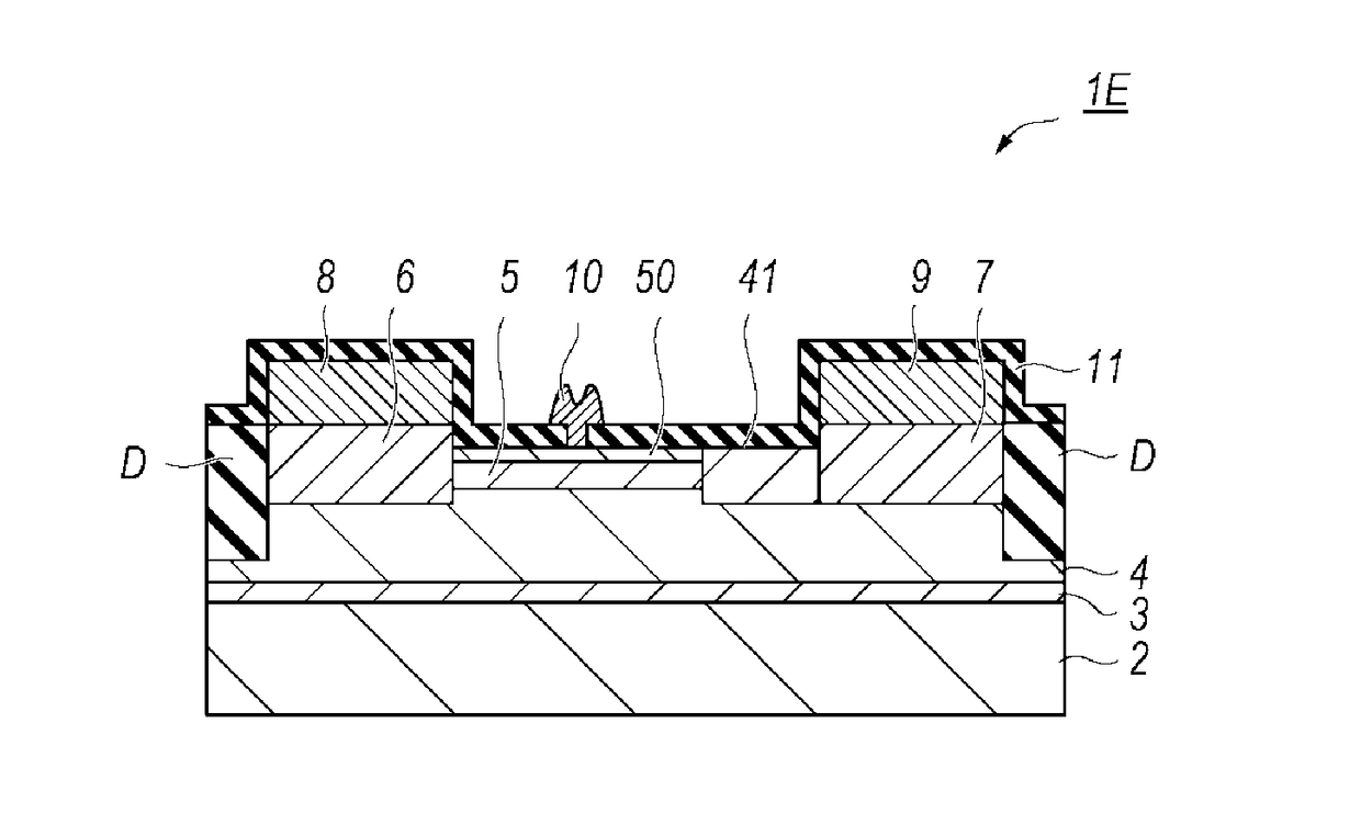
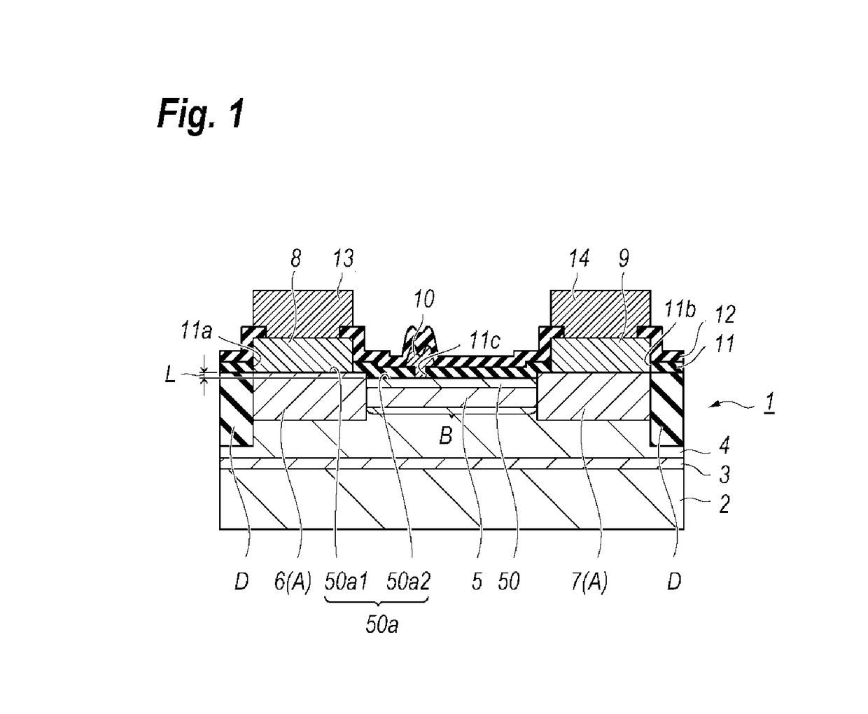
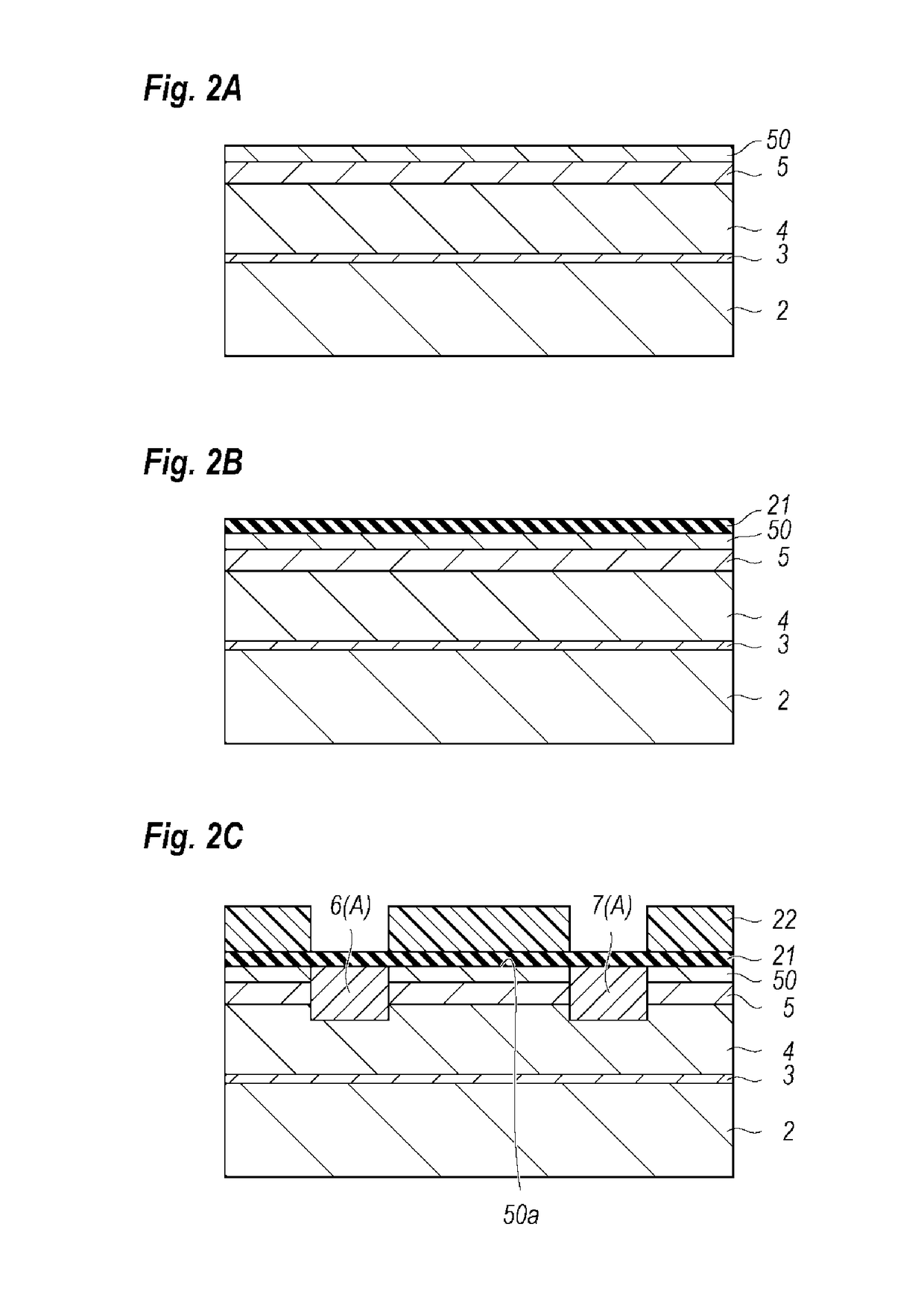
[0020]FIG. 1 shows a cross section of a semiconductor device according to the present inventions. The semiconductor device, which has a type of transistor of, what is called, a high electron-mobility transistor (HEMT), includes a substrate 2, a buffer layer 3, a channel layer 4, a barrier layer 5, a cap layer 50, n+ regions, 6 and 7, electrodes of a source 8, a drain 9, and a gate 10, and an insulating film 11. The HEMT 1 also provides a passivation film 12 that covers whole of the insulating film 11 and the electrodes 8 to 10. The source electrode 8 and the gate electrode 9 are connected to respective interconnections, 13 and 14, through openings formed in the pass...


PUM


Abstract

A process of forming a semiconductor device type of high electron-mobility transistor (HEMT) made of nitride semiconductor materials, and a HEMT formed thereby are disclosed. The process includes steps of implanting impurities into regions corresponding to n+ regions, activating the impurities by annealing, removing a disarranged region between the n+ regions, and forming the gate electrode onto the region where the disarranged region is removed in advance to the formation. The annealing, even when an insulating film covers the surface, causes the disarranged region primarily due to the sublimation of nitrogen (N). When the gate electrode is formed on the disarranged region, leak currents between the electrodes become substantial. Contrary, the HEMT of the invention provides the gate electrode onto a surface where the disarranged region is removed.

Description

BACKGROUND OF INVENTION[0001]1. Field of the Invention[0002]The present invention relates to a process of forming a nitride semiconductor device type of high electron mobility transistor (HEMT).[0003]2. Background Arts[0004]A semiconductor electron device using nitride semiconductor materials have been practically popular in a field because of superior breakdown voltages inherently attributed to the nitride semiconductor materials. A semiconductor device type of HEMT is widely used in the field. Recht; F et al., has reported in IEEE Electron Device Letters, vol. 27 (2006) pages 205 to 207, a HEMT having n+ regions beneath a source electrode and a drain electrode in order to improve contact resistance of those electrodes.[0005]The n+ regions may be formed by implanting ions accompanied with subsequent annealing at a temperature higher than 1000° C. in order to activate implanted ions. However, such annealing sometimes degrades the quality of the mother semiconductor materials to be p...

Claims


Application Information

Patent Timeline
IPC IPC(8): H01L29/778H01L21/324H01L29/66
CPCH01L29/7787H01L21/3245H01L29/66462H01L29/7786H01L29/0843H01L29/2003
Inventor KOYAMA, MASATOSHI
Owner SUMITOMO ELECTRIC IND LTD
Features
  • Generate Ideas
  • Intellectual Property
  • Life Sciences
  • Materials
  • Tech Scout
  • Unparalleled Data Quality
  • Higher Quality Content
  • 60% Fewer Hallucinations
Learn More