Eureka AIR delivers breakthrough ideas for toughest innovation challenges, trusted by R&D personnel around the world.

Multiple Gate Voltage Generation for FET Switches in Radio Frequency Circuits

Active Publication Date: 2017-05-04
PSEMI CORP
View PDF0 Cites 3 Cited by
  • Summary
  • Abstract
  • Description
  • Claims
  • Application Information

AI Technical Summary

Benefits of technology

The invention provides circuits and methods for selecting among multiple different positive and negative FET gate drive voltages for RF circuits. The circuits include multiple positive and negative voltage generators that can adjust the output voltage through adjusting the feedback signal or the reference voltage. The voltage generators can be connected to one or more level shifters to drive the gates of one or more FETs. The FET devices can be selectably coupled to the positive and negative voltage generators. The control signals for the voltage generators can be provided by the same IC or an external source. The invention allows for better tuning of gate drive voltages for optimal results in RF circuits.

Problems solved by technology

Typically, larger gate voltages allow for better RF characteristics (e.g., linearity, power handling capability), but can also lead to higher body leakage and to increased device stress, which can limit lifetime.
In some RF circuit applications utilizing such FET switch devices, there may be high and low performance channels.
Increased device stress reduces lifetime, and thus shortens testing time.
However, this has not been possible with fixed FET gate drive voltages.

Method used


Image

  • Multiple Gate Voltage Generation for FET Switches in Radio Frequency Circuits
  • Multiple Gate Voltage Generation for FET Switches in Radio Frequency Circuits
  • Multiple Gate Voltage Generation for FET Switches in Radio Frequency Circuits

Examples


Embodiment Construction

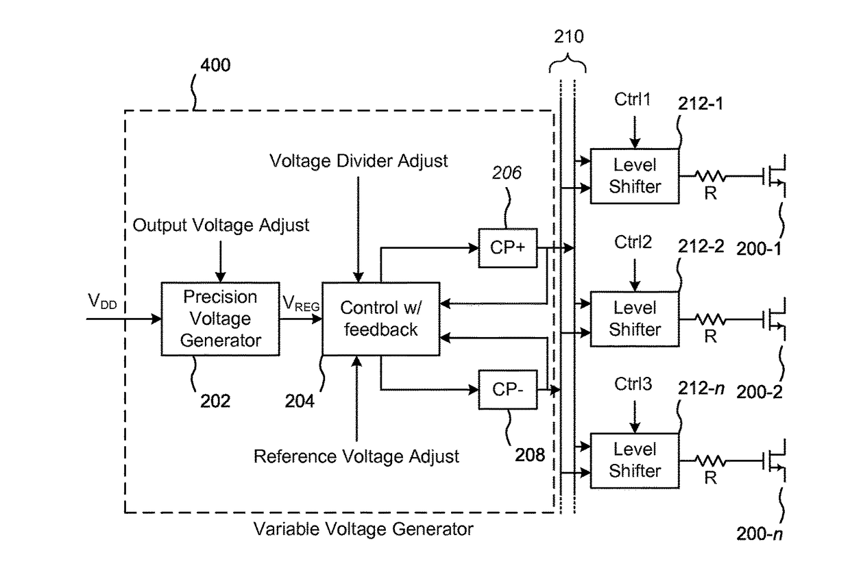
[0024]The invention encompasses circuits and corresponding methods that provide for selection among multiple different positive and / or multiple different negative FET gate drive voltages for FETs in which well-tuned gate drive voltages are needed or desirable for optimal results in an RF circuit, particularly an RF circuit manufactured with an SOI technology.

Context

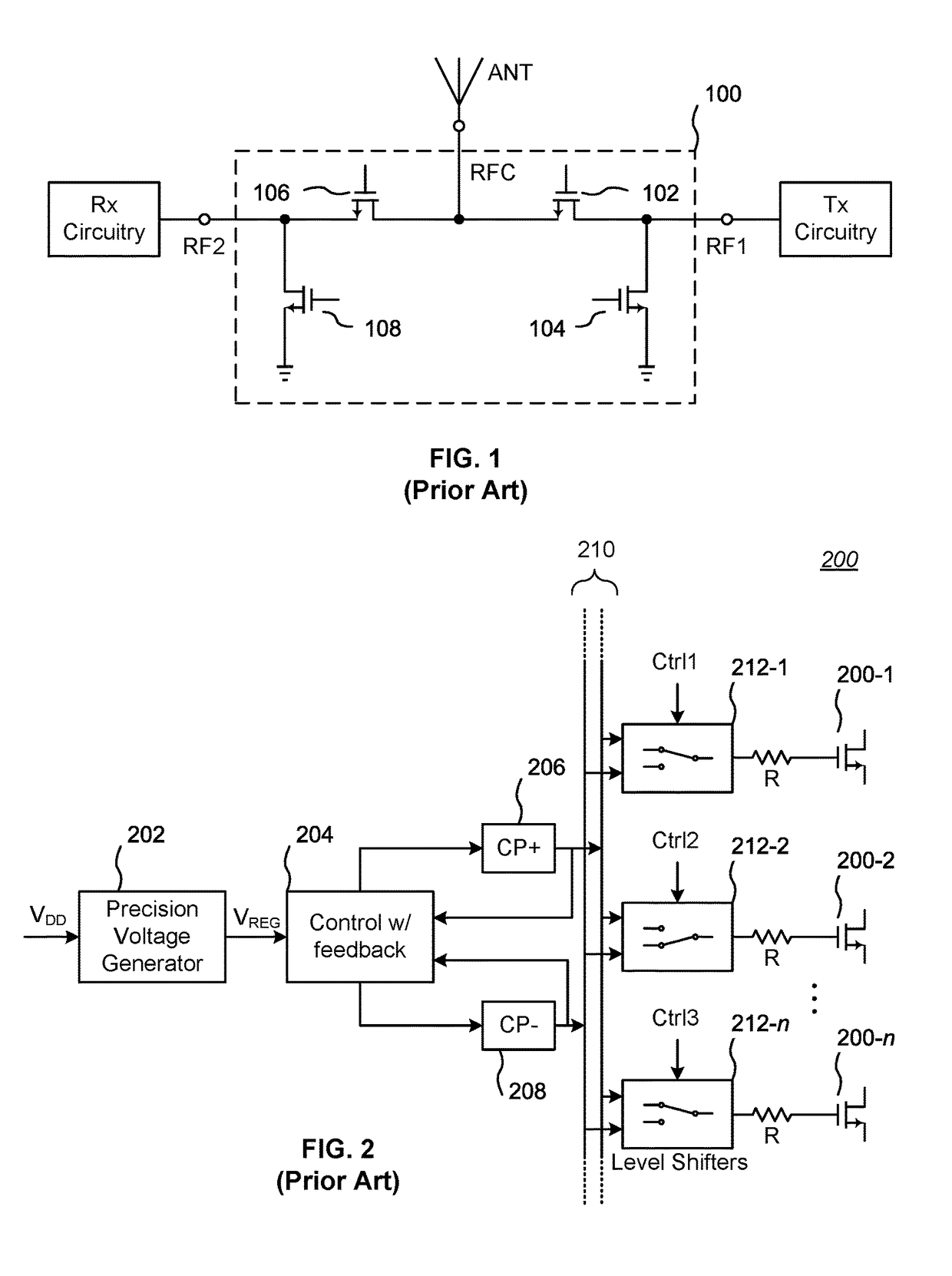
[0025]FIG. 1 is a schematic diagram of an RF switch circuit 100 in a transmit / receive circuit with FET switch devices defining signal paths. In this example, the RF switch circuit 100 has a port RFI coupled to transmitter circuitry Tx and a port RF2 coupled to receiver circuitry Rx. A common port RFC of the RF switch circuit 100 is shown coupled to an antenna ANT.

[0026]Signal propagation between the antenna ANT and either the transmitter circuitry Tx or the receiver circuitry Rx is controlled by the states of FETs 102 through 108. Signals pass between Tx and ANT when FET 102 is “ON” (conducting), FET 104 is “OFF” (non-con...


PUM


Abstract

Circuits and corresponding methods that provide for selection among multiple different positive and / or multiple different negative FET gate drive voltages for FETs in which well-tuned gate drive voltages are needed or desirable for optimal results in a radio frequency integrated circuit. Embodiments include FET gate drive variable voltage generator configurations which provide multiple different positive and / or multiple different negative FET gate drive voltages. In alternative embodiments, an IC may include multiple positive voltage generators and / or multiple negative voltage generators, each voltage generator providing an output voltage different from at least one other voltage generator. The voltage generators include charge pump based circuits and digital-to-analog converters. Each FET device requiring a well-tuned gate drive voltage is selectably coupled to at least one set of positive and negative voltage generators.

Description

BACKGROUND[0001](1) Technical Field[0002]This invention relates to electronic circuits, and more particularly to gate voltage generation circuits for field effect transistor switch devices in radio frequency circuits.[0003](2) Background[0004]Field effect transistors (FETs) are common circuit elements in modern electronic systems, and comprise a semiconductor body having a source, a drain, and a control gate. FETs may be fabricated in a number of integrated circuit (IC) technologies, such as the well-known standard bulk silicon, silicon-on-insulator (SOI) (including silicon-on-sapphire, or “SOS”), GaAs pHEMT, and MESFET IC technologies. One common use of field effect transistors (FETs) is as signal switching devices in radio frequency (RF) circuits.[0005]Not all FETs have the same electrical characteristics, which often vary by fabrication process. For example, SOI-based FETs for switching RF signals typically require well-tuned gate drive voltages for optimal results. Typically, la...

Claims


Application Information

Patent Timeline
IPC IPC(8): H03K17/687H02M3/07
CPCH03K17/6871H03K19/018507H03K19/018585H03K17/693
Inventor ENGLEKIRK, ROBERT MARK
Owner PSEMI CORP
Why Eureka
Eureka Blog
Learn More