Techniques for combining cmp process tracking data with 3D printed cmp consumables

a technology of process tracking and consumables, applied in additive manufacturing with liquids, semiconductor/solid-state device testing/measurement, additive manufacturing processes, etc., can solve the problems of non-uniform polishing of polishing pads manufactured by these methods, consumable components that are typically worn, and high cost and time consumption of manufacturing polishing pads

Active Publication Date: 2017-05-11
APPLIED MATERIALS INC
View PDF7 Cites 30 Cited by
  • Summary
  • Abstract
  • Description
  • Claims
  • Application Information

AI Technical Summary

Problems solved by technology

Polishing pads are consumable components that typically become worn after polishing a certain number of substrates.
These methods of manufacturing polishing pads are expensive and time consuming.
Moreover, polishing pads manufactured by these methods often yield non-uniform polishing results.
For example, during CMP, different areas on the substrate may be polished at different rates resulting in too much material removed (“overpolishing”) in some areas or too little material removed (“underpolishing”) in other areas.
In addition, polishing pads and other CMP apparatus manufactured by conventional techniques often lack devices and methods for performing various tracking, sensing, monitoring, and process metrology functions.
Conventional CMP systems often rely on system level sensing techniques which typically do not provide enough data to adequately control the CMP processes required to planarize devices formed in advanced technology integrated circuit nodes.

Method used


Image

  • Techniques for combining cmp process tracking data with 3D printed cmp consumables
  • Techniques for combining cmp process tracking data with 3D printed cmp consumables
  • Techniques for combining cmp process tracking data with 3D printed cmp consumables

Examples


process example

Additive Manufacturing Process Example

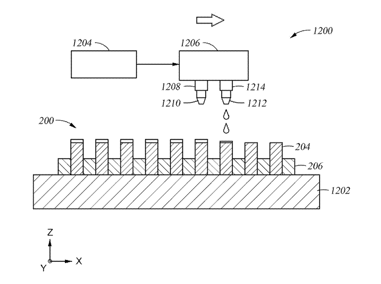
[0109]In one embodiment, 3D printing may be utilized to manufacture polishing pads, retaining rings, flexible membranes, and other CMP polishing apparatus components described herein. In one embodiment, the method of forming a 3D object may be performed by use of a CAD model of the components and use of a slicing algorithm that is used to map information about the components for every layer of the 3D object. A layer of the object may be formed by distributing a powder over the surface of a powder bed. A chosen binder material may then be deposited so as to selectively join particles where regions of the object are to be formed. An actuator (e.g., piston), which supports the powder bed and the components being manufactured, may be lowered in order for the next powder layer to be formed. After each layer is formed, the process is repeated followed by a final curing process (e.g., UV exposure or thermal treatment) to finalize a portion of the objec...


PUM

PropertyMeasurementUnit
distanceaaaaaaaaaa
elongation to breakaaaaaaaaaa
Tensile strengthaaaaaaaaaa

Abstract

Chemical mechanical polishing (CMP) apparatus and methods for manufacturing CMP apparatus are provided herein. CMP apparatus may include polishing pads, polishing head retaining rings, and polishing head membranes, among others, and the CMP apparatus may be manufactured via additive manufacturing processes, such as three dimensional (3D) printing processes. The CMP apparatus may include wireless communication apparatus components integrated therein. Methods of manufacturing CMP apparatus include 3D printing wireless communication apparatus into a polishing pad and printing a polishing pad with a recess configured to receive a preformed wireless communication apparatus.

Description

BACKGROUND[0001]Field[0002]Embodiments of the present disclosure generally relate to a chemical mechanical polishing (CMP) apparatus and methods of making and using the same. More specifically, embodiments described herein relate to techniques for collecting data in a CMP apparatus, such as collecting data relating to a CMP process and / or data relating to a component found in the CMP polishing apparatus.[0003]Description of the Related Art[0004]Chemical mechanical polishing (CMP) is a technique commonly used to planarize substrates during the fabrication of semiconductor devices. During a CMP process, a substrate being processed is mounted on a carrier head with the device surface positioned against a rotating polishing pad. The carrier head provides a controllable load to the substrate to push the device surface against the polishing pad. A polishing liquid, such as a slurry with abrasive particles, is typically supplied to the surface of the polishing pad. Polishing pads are consu...

Claims


Application Information

Patent Timeline
Patent Type & Authority Applications(United States)
IPC IPC(8): H01L21/67H01L21/66B24B37/26B29C67/00B24B49/14B24B49/16B24B49/10H01L21/306B24B49/00
CPCH01L21/67253B29L2031/736H01L22/20B24B37/26B24B49/003B24B49/14B24B49/16B24B49/10H01L21/67075B29C67/0055B33Y10/00B33Y80/00B29K2995/0003B29K2995/0005H01L21/30625H01L21/67294H01L22/12H01L22/26B29C64/106H01L21/304H01L21/67242H05K2201/10098
Inventor FUNG, JASON G.BAJAJ, RAJEEVREDFIELD, DANIELKHANNA, ANIRUDDHCORNEJO, MARIOMENK, GREGORY E.WATKINS, JOHN
Owner APPLIED MATERIALS INC
Why Eureka
Try Eureka