
Small wafer area MEMS switch

a micro-mechanicalelectronic switch and wafer area technology, applied in the direction of contacts, relays, coatings, etc., can solve the problems of inability to restore the switch to its original state when desired, inconvenient integration with state-of-the-art integrated circuits, and inefficient length

Inactive Publication Date: 2017-06-15
IBM CORP
View PDF0 Cites 3 Cited by
  • Summary
  • Abstract
  • Description
  • Claims
  • Application Information

AI Technical Summary

Benefits of technology

The present invention relates to a MEMS switch that is integrated into a vertical cavity in a silicon wafer. The switch uses a deep via technology to create a vertical cantilever that acts as a deflection electrode and a stationary electrode. The switch is small in size and can be used in a variety of applications. The invention also includes a method for manufacturing the MEMS switch using a damascene structure and a dielectric layer. The technical effects of the invention include a compact size, high reliability, and low power consumption.

Problems solved by technology

This uses a substantial wafer area, especially since RF chips are usually small.
Such devices, however, present many problems because their structure and innate material properties require that they be manufactured in lines that are separate from conventional semiconductor manufacture processing.
This is usually due to materials and processes which are incompatible and which cannot be integrated within existing semiconductor fabrication lines.
However, the MEMS must be provided with a low actuation-voltage switch and must not suffer from stiction, that is, the inability to restore the switch to its original state when desired.
An example of a MEMS found in the prior art requires a flexible silicon cantilever around 100 μm long, and typically requires 10 to 100 V operating voltage, which is unsuited for integration with state-of-the-art integrated circuits.
This length is inefficient as it occupies a substantial wafer area, especially since RF chips are usually small.
This design also requires a relatively high voltage.
In order to change the state of the switch, each time 20 mA current must be applied, which is not practical for a CMOS chip environment.
High-currents of this magnitude are not suitable for CMOS applications.
To date, conventional MEMS switches are not CMOS compatible because: (1) they are difficult to integrate using MOS process steps and, (2) they require a high-current and high actuation operation voltages.

Method used


Image

  • Small wafer area MEMS switch
  • Small wafer area MEMS switch
  • Small wafer area MEMS switch

Examples


embodiment

An Alternate Embodiment

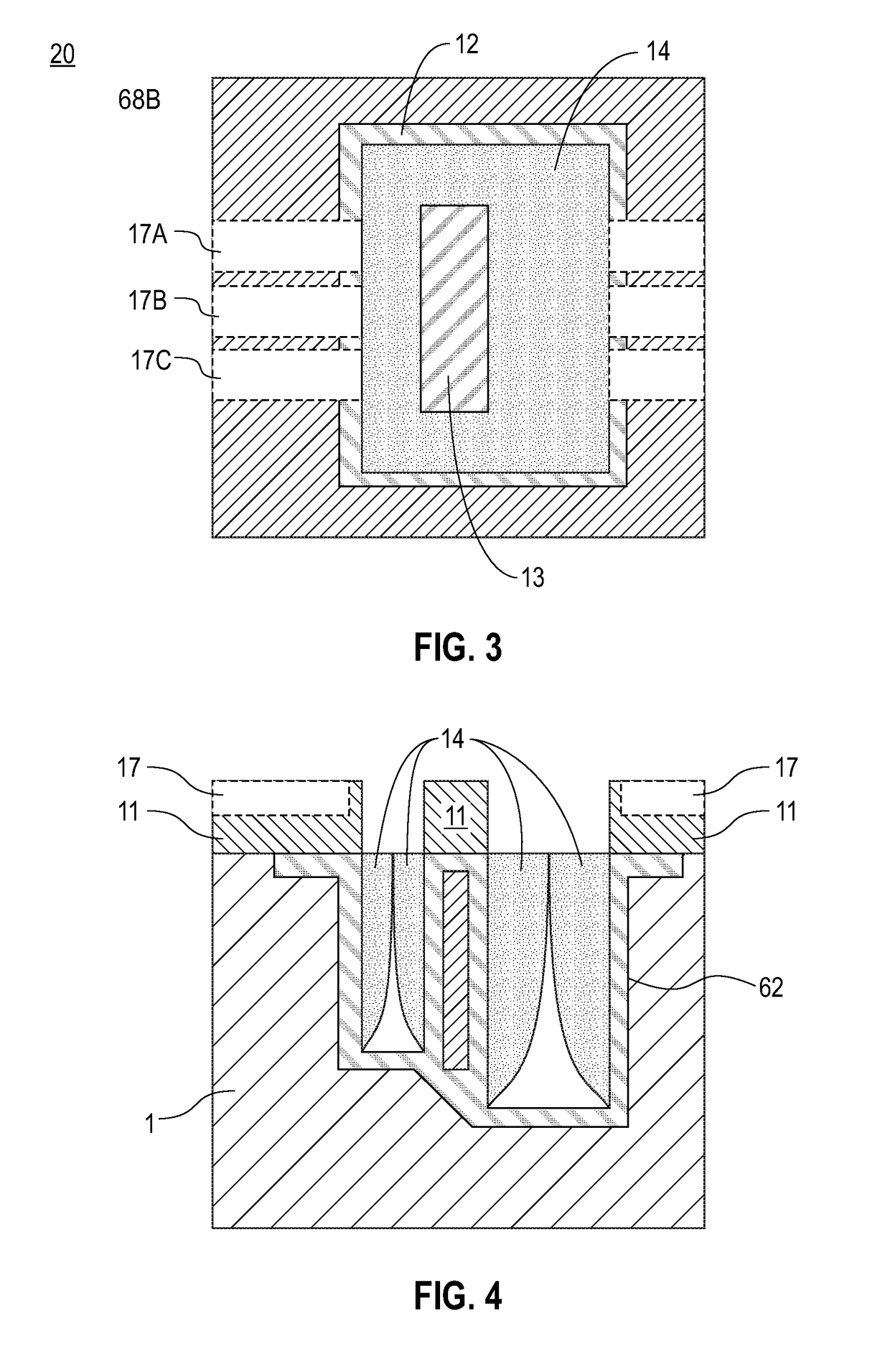
[0125]The other embodiment of the present invention comprises a MEMS switch as described hereinafter integrally coupled with a single or dual damascene structure thus forming a single unit.

[0126]In this embodiment, tungsten fill in each of the several trenches etched out of the silicon component serves as deflection, stationary and drive electrodes.

[0127]The advantage of the tungsten process is that the tungsten makes the electrodes from the start and there is no need to add any additional materials in the trenches later. One only needs to create contacts at the wafer surface to the tungsten to obtain a finished MEMS switch.

[0128]A dual damascene structure comprises a first etch-stop layer, a first dielectric layer, a second etch-stop layer, and a second dielectric layer. Before copper processes inside the dual damascene structure above the copper metal layer are performed, a barrier layer has to be formed to prevent copper atoms from diffusing into surroundin...


PUM

PropertyMeasurementUnit
Thicknessaaaaaaaaaa
Dielectric polarization enthalpyaaaaaaaaaa
Electrical conductivityaaaaaaaaaa

Abstract

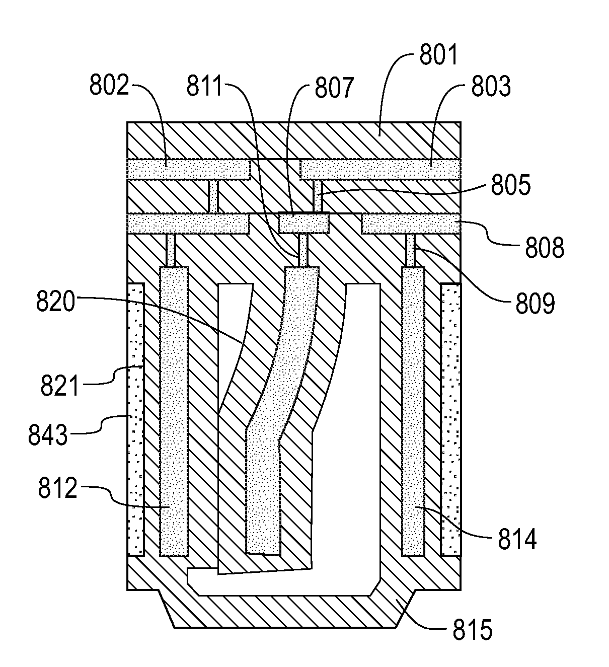
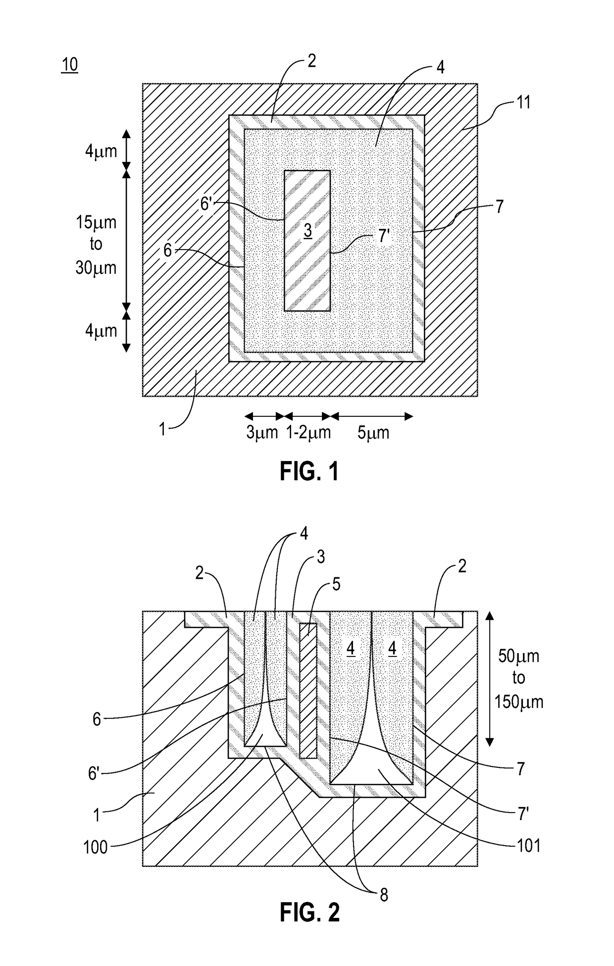
Deep via technology is used to construct an integrated silicon cantilever and cavity oriented in a vertical plane which creates an electrostatically-switched MEMS switch in a small wafer area. Another embodiment is a small wafer area electrostatically-switched, vertical-cantilever MEMS switch wherein the switch cavity is etched within a volume defined by walls grown internally within a silicon substrate using through vias.

Description

FIELD OF THE INVENTION[0001]The present invention relates to silicon integrated miniature micromechanical-electronic switches (MEMS) designed for R.F. receiver / transmitter systems especially for antenna and transmit / receive selection.DESCRIPTION OF THE PRIOR ART[0002]MicroElectroMechanical Systems (MEMS) are the integration of mechanical elements, sensors, actuators and electronics on a common substrate using integrated circuit process sequences. The electronics are fabricated using standard IC.[0003]More specifically, MEMS switches are surface-micromachined devices which use a mechanical movement to achieve a short circuit or an open circuit in a RF transmission-line. RF MEMS switches are specific micromechanical switches which are designed to operate at RF to mm-wave frequencies (0.1 to 100 GHz). The actuation forces required for the mechanical movement can be obtained using electrostatic, magneto-static, piezoelectric or thermal designs. The present invention is an electrostatic-...

Claims


Application Information

Patent Timeline
IPC IPC(8): B81B3/00B81C1/00
CPCB81B3/0056B81C1/00619B81B2201/012B81B2203/0118B81C2201/0178B81B2203/04B81B2207/07B81C2201/0132B81B2203/0315B81C1/0015H01H59/0009B81B2201/014B81C2201/0112B81C2203/0109B81C2203/0136H01H2001/0078
Inventor WEBB, BUCKNELL C.
Owner IBM CORP
Learn More