Photopatternable Silicones For Wafer Level Z-Axis Thermal Interposer

a technology of thermal interposers and silicones, which is applied in the direction of photomechanical devices, instruments, photosensitive material processing, etc., can solve the problems of increasing thermal challenges, increasing power consumption and consequent heat generation in semiconductor device packages, and limiting the use of tims

Inactive Publication Date: 2017-07-13
DOW SILICONES CORP
View PDF4 Cites 10 Cited by
  • Summary
  • Abstract
  • Description
  • Claims
  • Application Information

AI Technical Summary

Benefits of technology

[0002]Semiconductor devices are becoming smaller and more powerful. Semiconductor devices with high operating frequencies and large numbers of components with complex circuit densities are being fabricated with smaller packages, leading to increasing thermal challenges. High operating frequencies increase power consumption and consequently heat generation in a semiconductor device package. Typically, cooling hardware such as fans and heat sinks are used to dissipate the heat generated by the semiconductor device and cool the device. However, transfer of heat from the hot components in the semiconductor device package to the cooling hardware is may also be provided to significantly cool the semiconductor device.
[0005]Furthermore, the use of fillers in TIMs makes desirable careful management of the filler technology to prevent settling of fillers, as well as proper handling and dispensing of filled composites, forming uniform bond lines, and the like. These considerations further complicate the task of making a reliable low cost semiconductor device package module. Typically, the reverse side of most active semiconductor devices are rough, leading to air pockets and high thermal contact resistance between the TIM and the device thus reducing the effectiveness of the TIM.
[0008]U.S. patent application publication no. US20060006526 mentions a multilayered thermal interposer having two conductors bonded to an insulating layer with a bonding layer. However, the multiple layers of the thermal interposer make the manufacturing of the interposer and the semiconductor device package more complex.
[0011]WO2012 / 142592 recites a silicon interposer with through package vias. The silicon interposer comprises a silicon substrate in panel or wafer form having through package vias defined therein and redistribution layers on first and second sides of the silicon substrate simultaneously. However, the silicon interposer of WO2012 / 142592 is designed to reduce electrical losses within a semiconductor package thereby necessitating the use of a silicon wafer as the interposer. Moreover, the method of making the silicon interposer involves drilling or laser ablation of the wafer to create through package vias within the silicon wafer and further forming polymeric liners within the through package vias.

Problems solved by technology

Semiconductor devices with high operating frequencies and large numbers of components with complex circuit densities are being fabricated with smaller packages, leading to increasing thermal challenges.
High operating frequencies increase power consumption and consequently heat generation in a semiconductor device package.
However, hitherto applications of TIMs take place on die levels, thereby limiting the use of TIMs.
Thus there is a general limitation on the effectiveness of TIMs as a heat transport medium.
These considerations further complicate the task of making a reliable low cost semiconductor device package module.
Typically, the reverse side of most active semiconductor devices are rough, leading to air pockets and high thermal contact resistance between the TIM and the device thus reducing the effectiveness of the TIM.
The use of two plates and the hermetic bonding of the two plates make the interposer complex to manufacture.
However, the multiple layers of the thermal interposer make the manufacturing of the interposer and the semiconductor device package more complex.
However, to accommodate additional area of the thermal interposer that extends beyond the footprint of the die, a bigger semiconductor device package is desired, thus limiting the use of the thermal interposer and rendering the thermal interposer unusable when fabricating smaller packages.

Method used


Image

  • Photopatternable Silicones For Wafer Level Z-Axis Thermal Interposer
  • Photopatternable Silicones For Wafer Level Z-Axis Thermal Interposer
  • Photopatternable Silicones For Wafer Level Z-Axis Thermal Interposer

Examples


Embodiment Construction

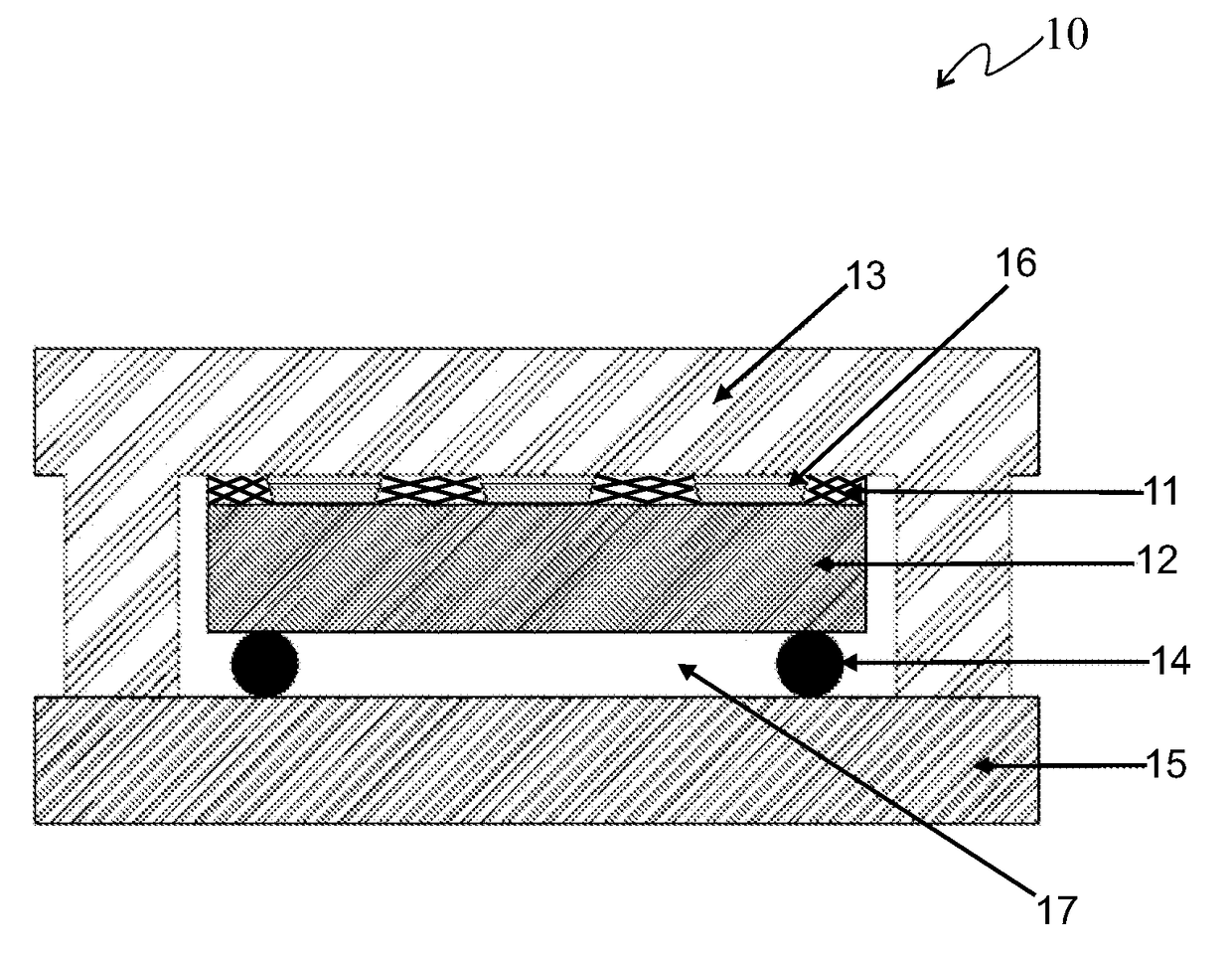
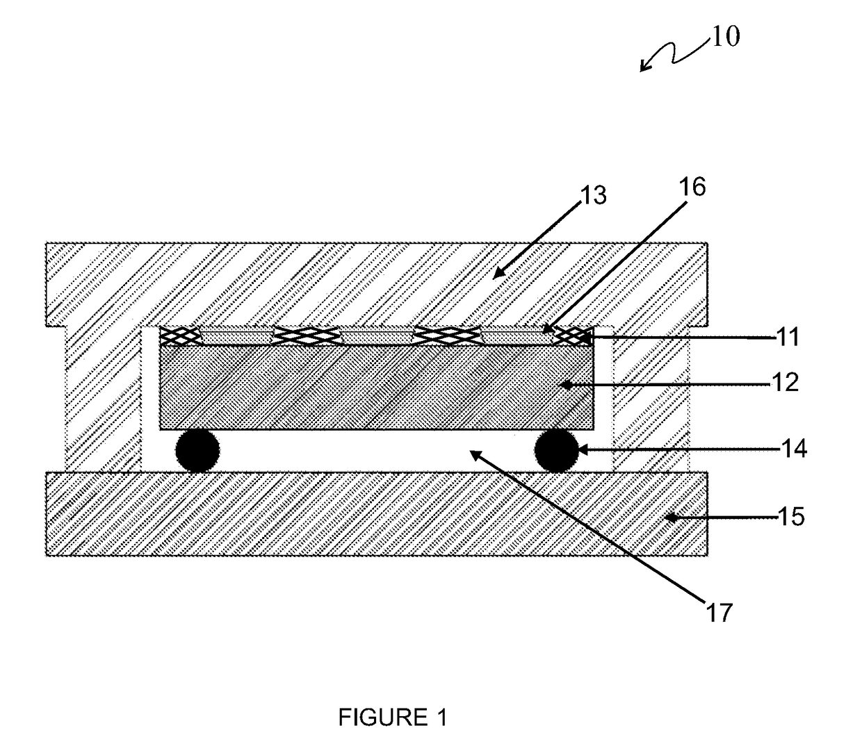
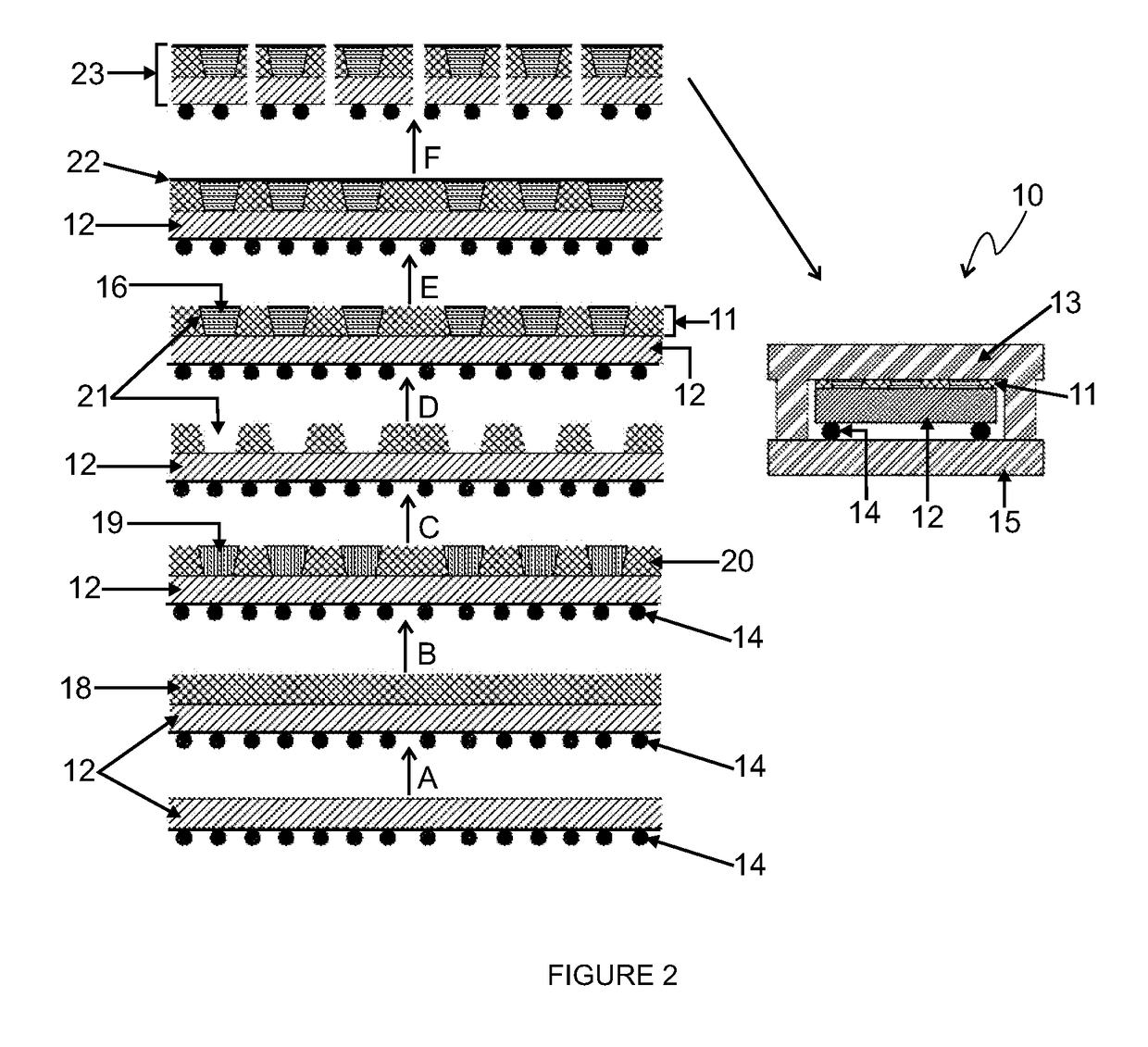
[0024]As used herein, “may” confers a choice, not an imperative. “Optionally” means is absent, alternatively is present. “Contacting” means bringing into physical contact. “Operative contact” comprises functionally effective touching, e.g., as for modifying, coating, adhering, sealing, or filling. The operative contact may be direct physical touching, alternatively indirect touching. All U.S. patent application publications and patents referenced herein, or a portion thereof if only the portion is referenced, are hereby incorporated herein by reference to the extent that incorporated subject matter does not conflict with the present description, which would control in any such conflict. All states of matter are determined at 25° C. and 101.3 kPa unless indicated otherwise. All % are by weight unless otherwise noted. All wt % values are, unless otherwise noted, based on total weight of all ingredients used to synthesize or make the composition, which adds up to 100 wt %. Any Markush ...


PUM

PropertyMeasurementUnit
temperatureaaaaaaaaaa

Abstract

Methods for fabrication of thermal interposers, using a low stress photopatternable silicone are provided, for use in production of electronic products that feed into packaging of LEDs, logic and memory devices and other such semiconductor products where thermal management is desired. A photopatternable silicone composition, thermally conductive material and a low melting point compliant solder form a complete semiconductor package module. The photopatternable silicone is applied on a surface of a wafer and selectively radiated to form openings which provided user defined bondline thickness control. The openings are then filled with high conductivity pastes to form high conductivity thermal links. A low melting point curable solder is then applied where the solder wets the silicone as well as the thermally conductive path that leads to low thermal contact resistance between the structured z-axis thermal interposer and the heat sink and / or substrate which can be a wafer or PCB.

Description

[0001]The present disclosure relates to photopatternable silicones and methods of forming interposers in semiconductor device packages using photopatternable silicone compositions.[0002]Semiconductor devices are becoming smaller and more powerful. Semiconductor devices with high operating frequencies and large numbers of components with complex circuit densities are being fabricated with smaller packages, leading to increasing thermal challenges. High operating frequencies increase power consumption and consequently heat generation in a semiconductor device package. Typically, cooling hardware such as fans and heat sinks are used to dissipate the heat generated by the semiconductor device and cool the device. However, transfer of heat from the hot components in the semiconductor device package to the cooling hardware is may also be provided to significantly cool the semiconductor device.[0003]Thermal Interface Materials (TIMs) are typically used as heat transport media between activ...

Claims


Application Information

Patent Timeline
Patent Type & Authority Applications(United States)
IPC IPC(8): H01L23/373H01L23/367H01L21/48H01L21/78C09K5/14G03F7/038G03F7/16G03F7/20G03F7/38G03F7/32H01L23/42C08G77/20
CPCH01L23/3737H01L23/42H01L23/3675H01L23/3736H01L21/4882H01L21/78C09K5/14G03F7/038G03F7/16G03F7/168G03F7/2002G03F7/38G03F7/32C08G77/20H01L23/3677H01L2924/0002G03F7/0755G03F7/0757G03F7/325G03F7/40C08G77/12C09D183/04H01L2924/00C08L83/00C08K5/56
Inventor JOHN, RANJITH SAMUELMEYNEN, HERMANYEAKLE, CRAIG R.
Owner DOW SILICONES CORP
Why Eureka
Try Eureka