Monocrystalline magneto resistance element, method for producing the same and method for using same

a monocrystalline magneto and resistance element technology, applied in the field of monocrystalline magneto resistance element, can solve the problems of low sensitivity as a magnetic sensor, disadvantageous recrystallization, low cost, etc., and achieve the effects of high interface flatness, low cost and mass productivity

Active Publication Date: 2017-08-10
NAT INST FOR MATERIALS SCI
View PDF3 Cites 16 Cited by
  • Summary
  • Abstract
  • Description
  • Claims
  • Application Information

AI Technical Summary

Benefits of technology

[0048]A monocrystalline magnetoresistance element according to an aspect of the present invention can provide a monocrystalline magnetoresistance element having a monocrystalline element with (001) orientation, similar to that on a MgO substrate on a Si substrate having a large diameter, and can provide a fundamental monocrystalline magnetoresistance element required for achieving mass productivity and low cost in order to apply a monocrystalline giant magnetoresistance ele

Problems solved by technology

However, when a general ferromagnetic body such as CoFe is used, a magnetoresistance (MR) ratio is about 3% (refer to Non-patent Literature 1), and a low sensitivity as a magnetic sensor is a problem.
However, an element utilizing a Heusler alloy electrode has such a serious problem that a high characteristic of a MR ratio of more tha

Method used


Image

  • Monocrystalline magneto resistance element, method for producing the same and method for using same
  • Monocrystalline magneto resistance element, method for producing the same and method for using same
  • Monocrystalline magneto resistance element, method for producing the same and method for using same

Examples


examples

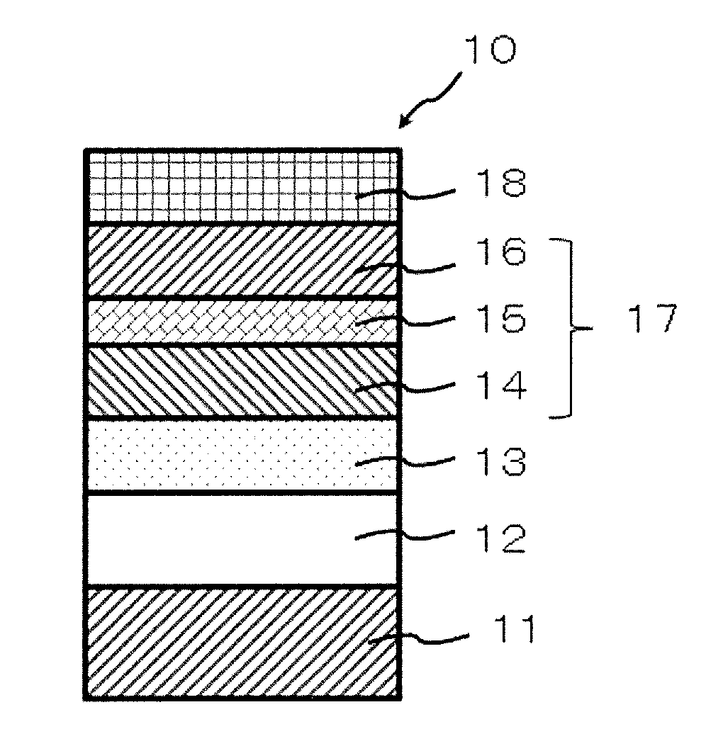
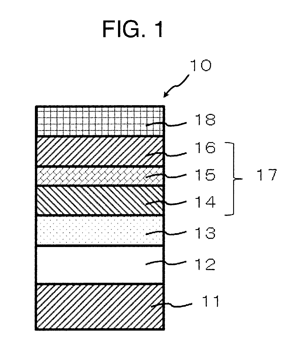
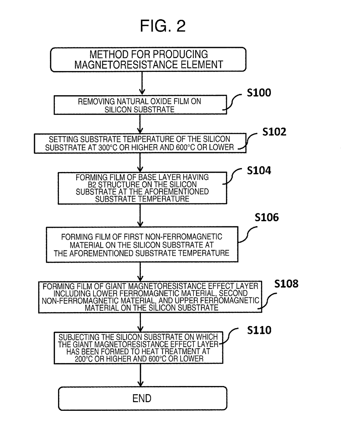
[0085]In a first Example, a film of NiAl (thickness 50 nm) having a B2 structure was formed on a Si(001) monocrystalline substrate from which a natural oxide film on a surface thereof had been removed with diluted hydrofluoric acid at a substrate temperature of 300° C. to 600° C.

[0086]FIG. 5 illustrates an XRD pattern of the NiAl thin film grown on the Si(001) substrate at the substrate temperature of 300, 400, 500, or 600° C. in an Example of the present invention, and a RHEED image thereof. The vertical axis indicates an intensity (count), and the horizontal axis indicates 20. As illustrated in FIG. 5, an X-ray diffraction pattern indicating single crystal growth of NiAl in a (001) direction and a streak of a reflection high energy electron diffraction (RHEED) image were observed at the substrate temperature of 400° C. to 600° C. On the other hand, an X-ray diffraction pattern indicating single crystal growth of NiAl in a (001) direction was not obtained but a peak in a (110) dire...


PUM


Abstract

To provide a key monocrystalline magnetoresistance element necessary for accomplishing mass production and cost reduction for applying a monocrystalline giant magnetoresistance element using a Heusler alloy to practical devices. A monocrystalline magnetoresistance element of the present invention includes a silicon substrate 11, a base layer 12 having a B2 structure laminated on the silicon substrate 11, a first non-magnetic layer 13 laminated on the base layer 12 having a B2 structure, and a giant magnetoresistance effect layer 17 having at least one laminate layer including a lower ferromagnetic layer 14, an upper ferromagnetic layer 16, and a second non-magnetic layer 15 disposed between the lower ferromagnetic layer 14 and the upper ferromagnetic layer 16.

Description

TECHNICAL FIELD[0001]The present invention relates to a magnetoresistance element having a ferromagnetic thin film preferably used as an electrode material of a tunnel magnetoresistance element, a current-perpendicular-to-plane giant magnetoresistance element, or the like, particularly to a monocrystalline magnetoresistance element obtained by epitaxially growing a (001) plane of a ferromagnetic thin film on a Si monocrystalline substrate having a large diameter.[0002]In addition, the present invention relates to a device using the monocrystalline magnetoresistance element.BACKGROUND ART[0003]A ferromagnetic thin film of Fe, FeCo, or the like is often used as an electrode material of a tunnel magnetoresistive (TMR) element or a current perpendicular to plane-giant magnetoresistance element. Many of these ferromagnetic materials have body-centered cubic lattice (bcc) structures. These magnetoresistance elements are used for a reproduction head of a hard disc drive (HDD) or a recordin...

Claims


Application Information

Patent Timeline
IPC IPC(8): H01L43/10H01L43/12H01F10/30H01L43/08H01F10/16H01F10/28
CPCH01L43/10H01F10/16H01L43/12H01F10/30H01L43/08H01F10/28H01F10/1936H01F10/3254H01F10/3272H10N50/10H10N50/01H10N50/85
Inventor CHEN, JIAMINSAKURABA, YUYALIU, JUNSUKEGAWA, HIROAKIHONO, KAZUHIRO
Owner NAT INST FOR MATERIALS SCI
Why Eureka
Try Eureka