Current induced spin-momentum transfer stack with dual insulating layers

a technology of memory transfer and current induced spin, which is applied in the field of current induced spin-momentum transfer stack with dual insulating layers, can solve the problems of limiting the density of memory, slow device operation, memory operation errors, etc., and achieves the advantages of reliability, speed of operation, and power saving

Inactive Publication Date: 2017-08-17
NEW YORK UNIV
View PDF0 Cites 29 Cited by
  • Summary
  • Abstract
  • Description
  • Claims
  • Application Information

AI Technical Summary

Problems solved by technology

This cross-talk will limit the density of the memory and / or cause errors in memory operations.
Further, the magnetic fields generated by such wires are limited to about 0.1 Tesla at the position of the electrodes, which leads to slow device operation.
Importantly, conventional memory designs also use stochastic (random) processes or fluctuating fields to initiate the switching events, which is inherently slow and unreliable (see, for example, R. H. Koch et al., Phys. Rev. Lett. 84, 5419 (2000)).
However, the proposed mechanism was purely theoretical.
However, the proposed devices are slow and rely on fluctuating magnetic fields and stochastic processes to initiate magnetization switching.
Further, large current densities are needed to switch the devices.
A disadvantage of the common collinearly magnetized STT-MRAM devices is that they often have long mean switching times and broad switching time distributions.
Relying on thermal fluctuations leads to incoherent reversal with an unpredictable incubation delay, which can be several nanoseconds.
However, the devices proposed were unreliable, as there was little consistency with regard to device characteristics.

Method used


Image

  • Current induced spin-momentum transfer stack with dual insulating layers
  • Current induced spin-momentum transfer stack with dual insulating layers
  • Current induced spin-momentum transfer stack with dual insulating layers

Examples


example 1

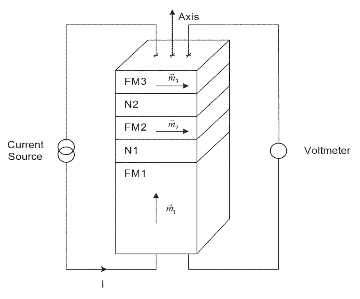
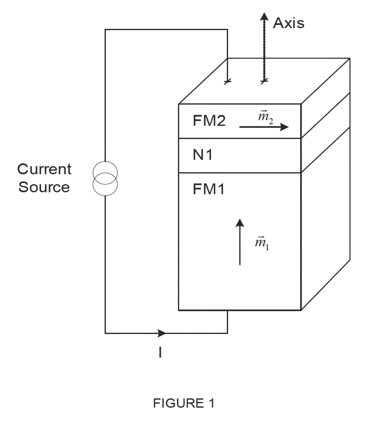
[0181]The OST-MRAM layer stack was grown on 150 mm oxidized silicon wafers using a Singulus TIMARIS PVD module. The device layer structure is illustrated in FIG. 21(a). The polarizer consists of a Co / Pd multilayer exchange coupled to a Co / Ni multilayer. The Co / Ni multilayer has a high spin polarization due to the strong spin-scattering asymmetry of Co in Ni and a perpendicular magnetic anisotropy (PMA). To enhance the layer coercivity and remanence this layer is coupled to Co / Pd which has a very large PMA but a lower spin polarization due to the strong spin-orbit scattering by Pd. The polarizer is separated by 10 nm of Cu from an in-plane magnetized CoFeB free layer that is one of the electrodes of a MTJ. The MTJ structure is 3 CoFeB|0.8 MgO|2.3 Co0.4 Fe0.4B0.2|0.6 Ru|2 Co0.4 Fe0.3 16 PtMn (number to the left of each composition indicates the layer thicknesses in nm). The wafer was annealed at 300° C. for 2 hours in a magnetic field and then characterized by vibrating sample magneto...

example 2

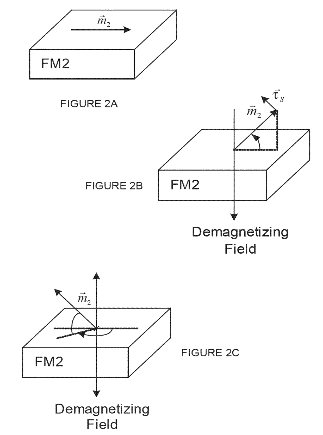
[0188]The magnetization dynamics of the device and method in the preferred embodiment can be modeled to a first approximation by considering the spin transfer torques associated with the perpendicular polarizer and the reference layer as follows:

dm^dt=-γμ0m^×H→eff+αm^×dm^dt+γaJm^×(m^×m^p)-βγaJm^×(m^×m^R)(2)

where m represents the magnetization direction of the free layer (it is a unit vector in the direction of the free layer magnetization). α is the damping parameter of the free layer. The prefactor, aJ, depends on the current density J, the spin-polarization P of the current density J, and the cosine of the angle between the free and pinned magnetic layers, cos(θ), such that aJ=Jg(P, cos(θ)) / (eMt). The is the reduced Planck's constant, g is a function of the spin-polarization P and cos(θ), M is the magnetization density of the free layer, e is the charge of an electron, and t is the thickness of the free layer. The last two terms are the spin transfer from the perpendicular polari...

example 3

[0193]In certain embodiments the reliable writing in which pulse duration is not critical. In such a case, for a memory operation, it may be preferable that the pulse duration not be a critical variable (i.e. the precise pulse duration would not determine the bit cell final state; only the pulse polarity—positive or negative—would be important. In this case, the device is provided with about equal to or greater than 1. This can be accomplished in a number of ways:

[0194]The spin-polarization from the reference layer can be increased by choice of materials for the magnetic tunnel junction and reference layer. For example, CoFeB in contact with MgO has a large spin-polarization. Permalloy (NiFe) in contact with MgO has a lower spin polarization.

[0195]The spin-polarization from the polarizing layer can be reduced. This can be accomplished in a number of ways, for example, without limitation:[0196]a. Choice of materials for the composition of the polarizing layer: Co / Ni multilayers have ...


PUM


Abstract

A high speed, low power method to control and switch the magnetization direction of a magnetic region in a magnetic device for memory cells using spin polarized electrical current. The magnetic device comprises a pinned magnetic layer, a reference magnetic layer with a fixed magnetization direction and a free magnetic layer with a changeable magnetization direction. The magnetic layers are separated by insulating non-magnetic layers. A current can be applied to the device to induce a torque that alters the magnetic state of the device so that it can act as a magnetic memory for writing information. The resistance, which depends on the magnetic state of the device, can be measured to read out the information stored in the device.

Description

CROSS-REFERENCE TO RELATED PATENT APPLICATIONS[0001]This application is a continuation of U.S. patent application Ser. No. 14 / 792,753, filed Jul. 7, 2015, now U.S. Pat. No. 9,449,668, which is a continuation of U.S. patent application Ser. No. 14 / 264,685, filed on Apr. 29, 2014, now U.S. Pat. No. 9,236,103, which is a continuation of U.S. patent application Ser. No. 13 / 298,190, filed Nov. 16, 2011, now U.S. Pat. No. 8,755,222, which claims the benefit of U.S. Provisional Application No. 61 / 414,724 filed Nov. 17, 2010. U.S. patent application Ser. No. 13 / 298,190 is also a continuation-in-part of U.S. patent application Ser. No. 13 / 041,104, filed Mar. 4, 2011, now U.S. Pat. No. 8,363,465, which is a divisional application of U.S. patent application Ser. No. 12 / 490,588, filed Jun. 24, 2009, now U.S. Pat. No. 7,911,832, which is a continuation-in-part of Ser. No. 11 / 932,745, filed Oct. 31, 2007 now U.S. Pat. No. 7,573,737. All of these applications are incorporated herein by reference i...

Claims


Application Information

Patent Timeline
Patent Type & Authority Applications(United States)
IPC IPC(8): G11C11/16H01L43/10H01L43/08H01L27/22
CPCG11C11/161G11C11/1653G11C11/1697H01L43/08G11C11/1673H01L27/226H01L43/10G11C11/1675H10N50/10
Inventor KENT, ANDREWBEDAU, DANIELLIU, HUANLONG
Owner NEW YORK UNIV
Why Eureka
Try Eureka