Thin optical system and camera

a technology of optical systems and cameras, applied in the field of thin, lightweight optics and camera modules, can solve the problems of insufficient room available for variable magnification (zoom), extreme limitations on the capabilities of camera modules used, and insufficient practical diameter and focal length of lenses, etc., to achieve high scan rates, low power requirements, and low cost

Inactive Publication Date: 2017-08-24
FISKE ORLO JAMES
View PDF7 Cites 116 Cited by
  • Summary
  • Abstract
  • Description
  • Claims
  • Application Information

AI Technical Summary

Benefits of technology

[0014]A camera module includes a miniature scanning mirror and lens assembly disposed along the optical path of the system. The scan mirror design provides tiny package dimensions, high scan rates, low power requirements and low cost. The lens elements correspond to thin lateral slices taken from the center of circular lenses, and focus an image segment onto an imaging sensor. The term scan mirror, mirror segment, and scan mirror segment are used interchangeably herein and refer to the mirror structure of the present invention. The imaging sensor corresponds to a thin slice taken from a rectangular image sensor. As the scanning mirror pivots on one axis to scan the scene of interest, the imaging sensor captures successive image segments. Multiple image segments are stitched together by software running on a digital processor to provide a complete image. The lens assembly may include moveable elements to allow variable focus and variable magnification, and may utilize refraction, reflection, diffraction and / or planar optical elements. The camera module may be less than 5 millimeters thick while allowing long focal length lenses and far more light collecting area than previously possible in a camera of this thickness. Other embodiments include a switchable scan mirror with two apertures and a dual-camera system that provides binocular images and video.

Problems solved by technology

This places extreme limitations on the capabilities of the camera modules used, since the short optical path from the front of the lens to the image sensor severely restricts the practical diameter and focal length of the lens.
The entrance pupil of the lens may be less than 2 millimeters, providing just 3 square millimeters of light collecting area or less, and insufficient room is available to allow variable magnification (zoom).
These options result in more bulk and clearly undesirable aesthetics.
This approach adds cost and complexity, and is far less convenient than an integral lens.
This design allows a longer optical path than the design of FIG. 2, but with the unfortunate result that either the camera module must be thick enough to fit a lens of large enough diameter to provide good optical performance or the lens diameter must remain small, providing little performance improvement.
This may increase the final image resolution and in some cases provide magnification of up to perhaps four or five times, at the cost of more complex and expensive hardware, the need to develop highly sophisticated image processing algorithms and demanding computational requirements in the mobile device.
In comparison, some commonly available cameras include an integral zoom lens capable of optically magnifying an image by a factor of 40 to 60 times. Similar capability would be highly advantageous if it could be included in a low-cost camera module suitable for use in cell phones and other mobile devices, but none of the usual methods used to improve camera module capability are likely to ever come close to achieving this.
However, the placement of conductive loop 75 on top of mirror 74 adds fabrication steps and decreases the reflective area of the mirror, both of which increase the cost of a mirror of a specific size.
The need to constrain the width of the conductor used to form loop 75, and thereby minimize loss of mirror area, also creates relatively high current resistance through the loop, decreasing performance and making the scanning mirror less power efficient than is desirable.

Method used


Image

  • Thin optical system and camera
  • Thin optical system and camera
  • Thin optical system and camera

Examples


second embodiment

[0065]FIG. 15 is a section diagram of the magnets of MEMS mirror 110. In this embodiment, magnets 151a and 151b are appended to the ends of the magnet configuration of FIG. 14, which serves to further shape and constrain the magnetic field lobes. Again, other embodiments may use a single magnet with a multipole magnetization pattern that is substantially equivalent to that shown in FIG. 15 without straying from the intended scope of the present invention.

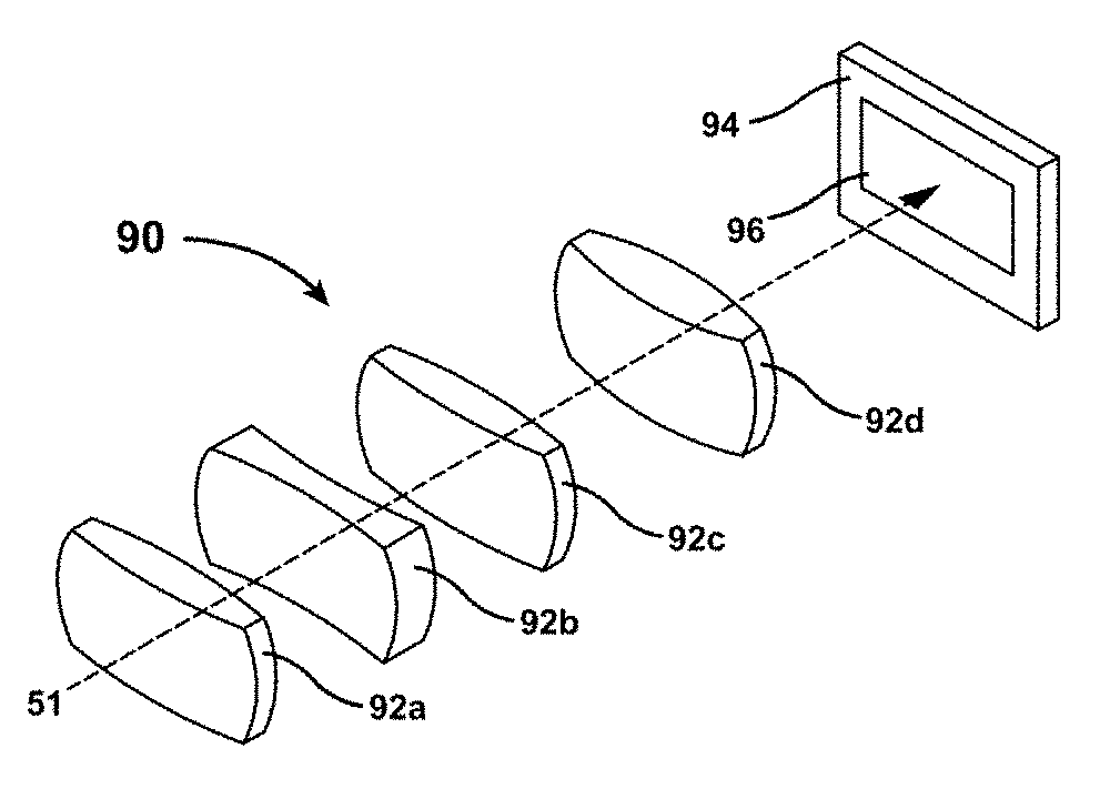
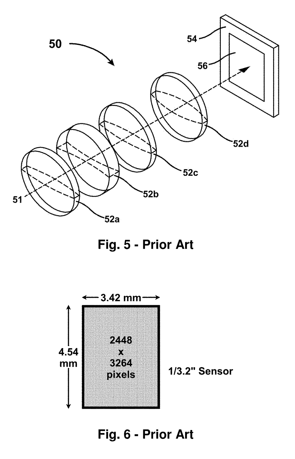
[0066]FIG. 16 depicts a section view of optical path 160 according to the present invention. Light rays 51 (shown by dotted lines throughout) enter through an entrance pupil 161 which is a lens or window that is long and narrow similar to the lens slices of optical path 100 in FIG. 9B.

[0067]Optical path 160 may also include a controllable shutter or variable neutral density filter 162, which may be placed in the position shown or elsewhere in the optical path, to vary the amount of light allowed or the depth of focus. Light rays 51 ...

first embodiment

[0073]FIG. 21 depicts the image scanning procedure used by camera module 170. With mirror segment 120 rotated to the designated scan limit in one direction, image sensor 165 captures a first image segment and transfers the first image segment to control processor 202. Control processor 202 then provides the appropriate current direction and amplitude through mirror segment 120 to rotate the mirror segment one third of the way toward the second designated scan limit, where image sensor 165 captures a second image segment and transfers the second image segment to control processor 202. This process repeats for image segments three and four, after which mirror segment 120 has reached the second designated scan limit from where mirror segment 120 started. Mirror rotation angle is precisely controlled and image segment capture is precisely timed such that each successive image segment overlaps the previous image segment to a small degree. In this first embodiment, scan mirror 120 pauses ...

embodiment 270

[0087]Embodiments of the present invention revealed thus far have all used a scanning element to collect light from directions centered roughly perpendicular to the optical path through the camera module lenses. FIG. 27 is a section view of thin camera module embodiment 270 that provides other features, including a configuration allowing a scanning element to collect light from directions centered roughly parallel to the optical path through the camera module lenses. Light rays 51 pass through lens or window 161, reflect from mirror segment 120, reflect from mirror prism 272, pass through movable lens elements 273a, 273b, and 273c, then reflect from mirror prism 172 and focus onto image sensor 165, which also is movable. In this embodiment lens elements 273a, 273b, and 273c are planar lenses, which provide extremely thin and lightweight lens elements with little or no chromatic aberration. This allows one very thin lens element to replace two or more thick lens elements usually requ...


PUM


Abstract

A camera module (170) includes a miniature scanning mirror (120), lens elements (163a to 163d) corresponding to thin lateral lens slices, and a short, wide imaging sensor (165). As the scanning mirror (120) pivots to scan a scene, the imaging sensor (165) captures successive image segments. Multiple image segments are stitched together by software running on a digital processor to provide a complete image. The assembly of lens elements (163a to 163d) may include moveable elements to allow variable focus, variable magnification and image stabilization, and may utilize refraction, reflection, diffraction and/or planar optical elements. The camera module (170) may be less than 5 millimeters thick while allowing long focal length lenses and increased light collecting area. Other embodiments include a switchable scan mirror with two apertures and a dual-camera system that provides binocular images and video.

Description

CROSS REFERENCE TO RELATED APPLICATIONS[0001]The present application is a continuation application of PCT Application Serial No. PCT / US2015 / 61285, filed 18 Nov. 2015, which claims priority from U.S. Provisional Application No. 62 / 081,909 filed on 19 Nov. 2014, the contents of which are herein incorporated by reference in its entirety.FIELD OF THE INVENTION[0002]This invention relates generally to optics and camera modules, and more particularly to thin, lightweight optics and camera modules for portable devices such as cameras, cellular telephones and the like.BACKGROUND OF THE INVENTION[0003]Pocket cameras have become ubiquitous, particularly in the form of cell phone cameras. FIG. 1 shows a cutaway view of a typical configuration of a cell phone 10. A miniature camera module 12, including a complete optical system, typically fits in a tiny package installed inside the cell phone case, as shown. Camera modules of this type are typically on the order of 8 millimeters wide, 8 millime...

Claims


Application Information

Patent Timeline
Patent Type & Authority Applications(United States)
IPC IPC(8): G02B13/00G02B26/10G02B26/08G02B7/02G02B7/182
CPCG02B13/0055G02B7/021G02B26/105G02B26/085G02B7/1821G02B13/001H04N23/57H04N23/55H04N23/60H04N23/69
Inventor FISKE, ORLO JAMES
Owner FISKE ORLO JAMES
Why Eureka
Try Eureka