Mixed organic-inorganic perovskite formulations

a technology of organic and inorganic perovskite, which is applied in the field of mixed organicinorganic perovskite formulations, can solve the problems of high cost of manufacturing devices that capture solar energy, high material cost, and historically impede the widespread use of solar energy, and achieve the ability to use these compounds

Active Publication Date: 2017-08-24
OXFORD PHOTOVOLTAICS
View PDF2 Cites 23 Cited by
  • Summary
  • Abstract
  • Description
  • Claims
  • Application Information

AI Technical Summary

Benefits of technology

[0016]Advantageously, substantially all of the starting materials will be consumed or eliminated in the production of the final perovskite with the particular selected phase, that is, substantially no unreacted starting materials will contaminate the final perovskite product. It is desirable that the by-products that will form are able to be removed using conditions that do not degrade final perovskite product. It will of further benefit that the present invention is straightforward and cost effective to perform.
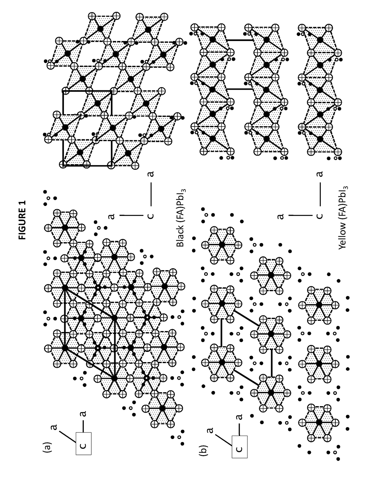
[0026]Not wishing to be bound by any particular theory, it is possible that the size of the A′ and X′ ions relative to the spacing between the atoms in the crystal lattice of the hybrid organic-inorganic perovskite, may be influential in choosing appropriate compounds to supply the A′ and X′ ions. Alternatively, the presence of the A′ and X′ may somehow hinder the crystallisation of the perovskite material in the phase which has the higher band gap, or conversely in some way encourage the crystallisation of the perovskite material in the phase which has the smaller band gap (i.e. below 3.0 eV). Thus, in the formulation of the present invention, the one or more second anions, A′ and / or the one or more second anions, X′ can interact with the nucleation and / or growth of the perovskite crystals to preferentially favour the formation of the particular chosen phase structure.

Problems solved by technology

To this end, solar energy is seen as one of the most promising technologies, nevertheless, the high cost of manufacturing devices that capture solar energy, including high material costs, has historically hindered its widespread use.
If the band gap is too high, most daylight photons cannot be absorbed; if it is too low, then most photons have much more energy than necessary to excite electrons across the band gap, and the rest will be wasted.
Unfortunately, the formation of these different phases becomes a significant problem to the ability to the use of these compounds when the temperature range over which the material transitions from one phase to another, is low, for example below 200° C.
Wide bandgap semiconductor but chain-like structure hinders electronic transport.
As a further difficulty, although phase transitions as a result of changing temperature are observed in the bulk powder materials, the same is not readily observed when the materials are formed in a thin film.
This one-step deposition process which is followed by a thermal cure, can be performed under either ambient or inert conditions, but in neither environment is free of problems and both cause difficulty when trying selectively to prepare the alpha-phase perovskite.
Another problem is that the delta-phase is the prominant material when the thin film product is formed on a meso-porous scaffold (e.g. zirconia or alumina structures).
A yet further problem with the one-step process is that the starting materials poorly convert to the perovskite and this results in the presence of PbI2 as an impurity in the product.
Unfortunately, increasing the FAI content only leads to poor formation and poor performance of the thin film due to the presence of unreacted FAI, and this material presents another difficulty in that it cannot be easily removed owing to its low volatility.
This two-step process not only has the disadvantage that it requires more than one step which increases the complexity and cost of the process, but it leads to a mixture of the alpha- and delta-phases.
Also, it can lead to poor conversion of the starting materials to the perovskite leaving unconverted PbI2 within the film which along with the delta-phase will typically decrease charge transport capabilities, as well as useful spectral absorption, and therefore will exhibit poorer cell performance.

Method used


Image

  • Mixed organic-inorganic perovskite formulations
  • Mixed organic-inorganic perovskite formulations
  • Mixed organic-inorganic perovskite formulations

Examples


examples

[0129]Materials.

[0130]In the exemplary embodiments detailed below, unless otherwise stated, all materials were purchased from Sigma-Aldrich or Alfa Aesar and used as received. Spiro-OMeTAD was purchased from Lumtec.

[0131]Perovskite precursor synthesis: Formamidinium iodide (FAI) were synthesised by dissolving formamidinium acetate powder in a 2× molar excess of 57% w / w hydroiodic acid (for FAI). After addition of acid the solution was left stirring for 10 minutes at 50° C. Upon drying at 100° C., a yellow-white powder is formed. This was then washed with diethyl ether and recrystallized twice with ethanol, to form white needle-like crystals. This was previously demonstrated by Eperon et al. Before use, it was dried overnight in a vacuum oven. The methylammonium iodide (MAI) was synthesised according to literature methods.

[0132]To form FAPbI3 precursor solutions, FAI, MAI and PbCl2 (or PbI2) were dissolved in anhydrous N,N-dimethylformamide (DMF) or dimethylsulfoxide, (DMSO) in the v...


PUM

PropertyMeasurementUnit
band gapaaaaaaaaaa
band gapaaaaaaaaaa
temperatureaaaaaaaaaa

Abstract

A formulation for use in the preferential formation of thin films of a perovskite material AMX 3 with a certain required crystalline structure, wherein said formulation comprises two or more compounds which between them comprise one or more first organic cations A; one or more metalcations M; one or more second cations A′; one or more first anions X and one or more second anions X′.

Description

FIELD OF THE INVENTION[0001]The present invention relates to a formulation suitable for making hybrid organic-inorganic perovskite compounds which have a particular preferred crystalline structure, and to a process for obtaining such hybrid organic-inorganic perovskites. The invention also relates to optoelectronic devices including photovoltaic devices such as solar cells and light-emitting devices, which use the formulation of the invention for making hybrid organic-inorganic perovskite compounds with a particular preferred crystalline structure.BACKGROUND OF THE INVENTION[0002]Over the past forty years or so there has been an increasing realisation of the need to replace fossil fuels with more secure sustainable energy sources. The new energy supply must also have low environmental impact, be highly efficient and be easy to use and cost effective to produce. To this end, solar energy is seen as one of the most promising technologies, nevertheless, the high cost of manufacturing d...

Claims


Application Information

Patent Timeline
Patent Type & Authority Applications(United States)
IPC IPC(8): H01G9/20H01L51/00H01L31/032C07C251/30
CPCH01G9/2009C07C251/30H01L51/0077H01L51/4226H01L31/032H01L2031/0344H01G9/2031C01G21/006C01P2002/34C01P2002/72C01P2006/90Y02E10/549Y02E10/542Y02P70/50H10K85/00H10K30/151H10K85/50H10K85/30
Inventor BEAUMONT, NICOLAKAMINO, BRETT AKIRALANGLEY, BENJAMINCROSSLAND, EDWARD JAMES WILLIAM
Owner OXFORD PHOTOVOLTAICS
Why Eureka
Try Eureka