Semiconductor device

a technology of semiconductors and devices, applied in the direction of semiconductor devices, basic electric elements, electrical equipment, etc., can solve problems such as complicated manufacturing processes, reduce the number of times of mask formation, reduce potential design errors, and reduce the complication of manufacturing processes

Active Publication Date: 2017-09-14
TOYODA GOSEI CO LTD
View PDF5 Cites 1 Cited by
  • Summary
  • Abstract
  • Description
  • Claims
  • Application Information

AI Technical Summary

Benefits of technology

[0086]In the configuration of the first embodiment, the first electrode 141 and the second electrode 144 are mainly made of the same metal. This enables the first electrode 141 and the second electrode 144 to be formed in one identical process. This reduces the complication in the manufacturing process.
[0087]When the first electrode 141 and the second electrode 144 are formed in different processes, mask formation using a photoresist is required multiple times. The embodiment, however, enables the first electrode 141 and the second electrode 144 to be formed in one identical process. This reduces the number of times of mask formation. As a result, this reduces a potential design error due to the frequency of mask formation and thereby allows for miniaturization of the semiconductor device.
[0088]In order to allow the first electrode 141 and the second electrode 144 to be mainly made of the same metal, the conditions are required to provide the ohmic contact with the n-type semiconductor region 116 and to provide the ohmic contact with the p-type semiconductor region 114. The following describes evaluation tests proving that the semiconductor device 100 of the embodiment satisfies these required conditions.
[0090]FIG. 8 is a sectional view schematically illustrating the structure of a semiconductor element 300 that was used in a first evaluation test. The XYZ axes similar to those of FIG. 1 are illustrated in FIG. 8. The semiconductor element 300 includes a substrate 310, a buffer layer 311, a semiconductor layer 312, a p-type semiconductor region 320, an n-type semiconductor region 330 and electrodes 341 and 344. The semiconductor element 300 is an element used to measure the contact resistance by a method based on a transmission line model (TLM).
[0103]In terms of providing the further lower contact resistance, “Nd—Na [cm−3]” is preferably not less than 1.7×1010 cm−3, is more preferably not less than 3.0×1010 cm−3, is furthermore preferably not less than 5.0×1010 cm−3, and is especially preferably not less than 1.0×1020 cm−3. In terms of suppressing the surface roughness of the semiconductor by ion implantation, on the other hand, “Nd—Na [cm−3]” is preferably not greater than 1.0×1021 cm−3 and is more preferably not greater than 4.0×1020 cm−3. The “concentration of Mg as p-type impurity (Na) [cm−3]” is preferably not lower than 1.0×1018 cm−3.

Problems solved by technology

This complicates the manufacturing process.

Method used


Image

  • Semiconductor device
  • Semiconductor device
  • Semiconductor device

Examples


first embodiment

A. First Embodiment

[0038]A-1. Structure of Semiconductor Device

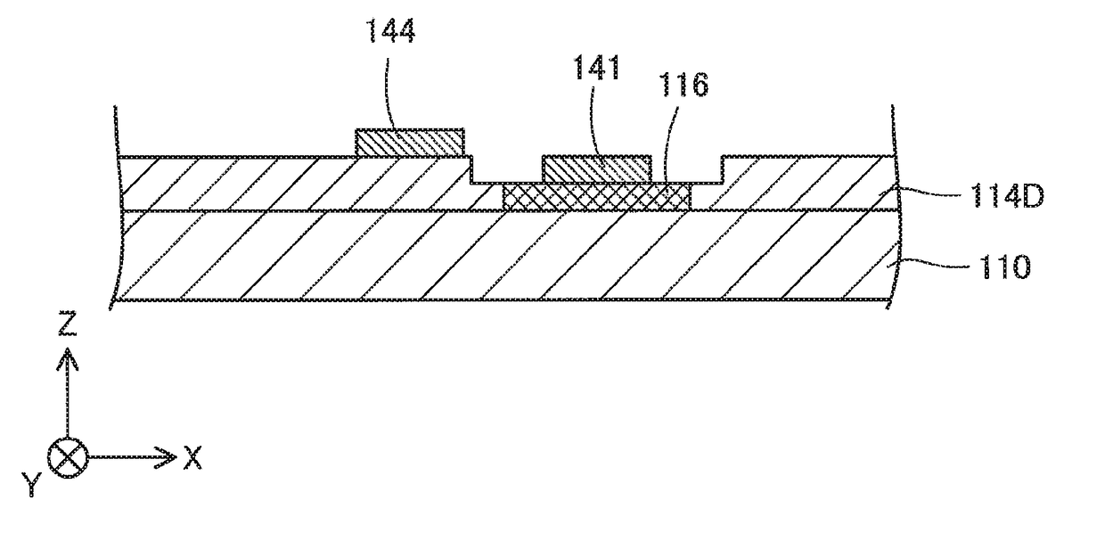
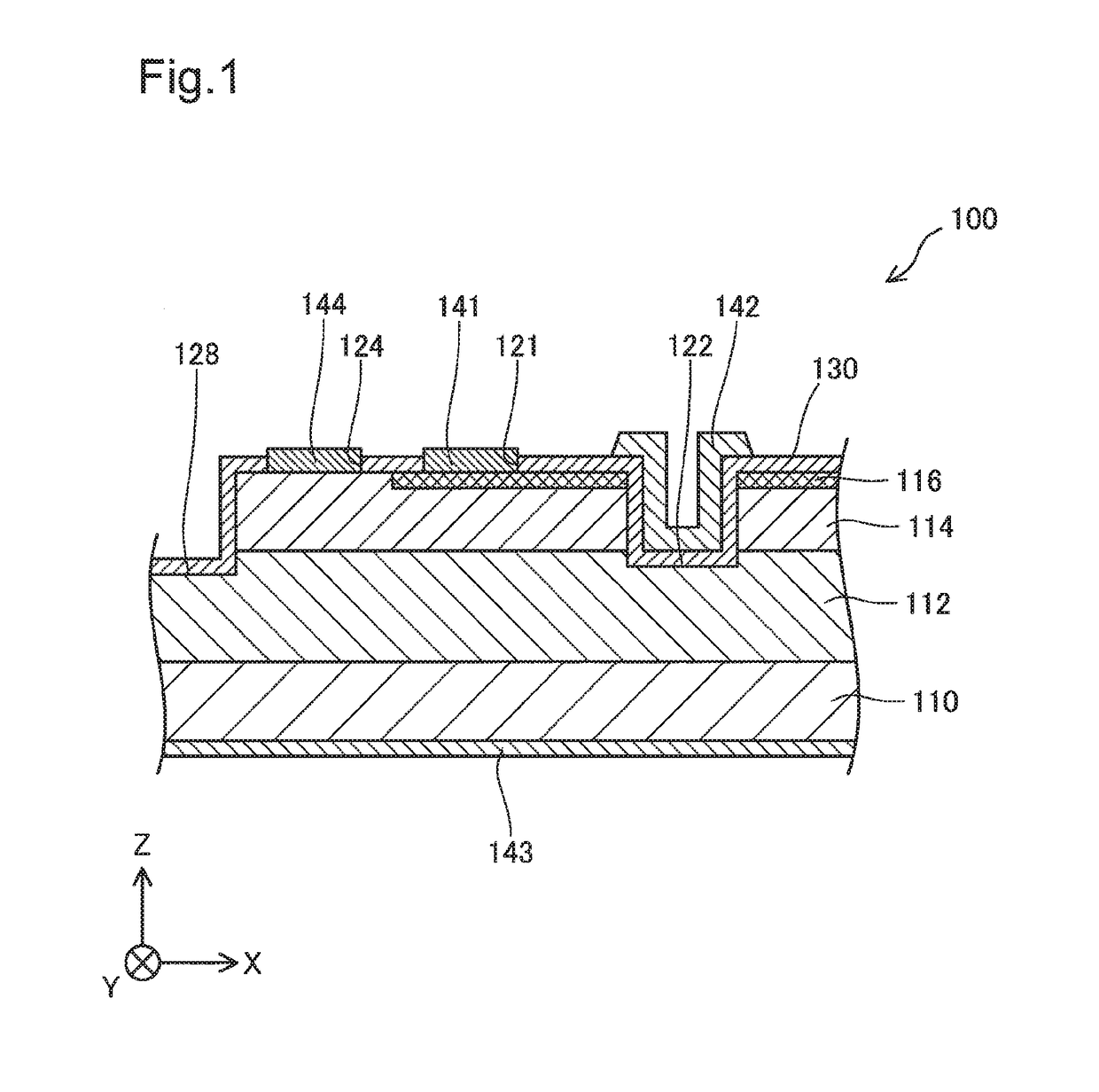
[0039]FIG. 1 is a sectional view schematically illustrating the structure of a semiconductor device 100 according to a first embodiment. The semiconductor device 100 is a GaN-based semiconductor device formed by using gallium nitride (GaN). According to this embodiment, the semiconductor device 100 is a vertical trench MOSFET (metal-oxide-semiconductor field-effect transistor). According to this embodiment, the semiconductor device 100 is used for power control and is also called power device.

[0040]XYZ axes orthogonal to one another are illustrated in FIG. 1. Among the XYZ axes of FIG. 1, the X axis denotes a left-right axis on the sheet surface of FIG. 1. +X-axis direction denotes a rightward direction on the sheet surface, and −X-axis direction denotes a leftward direction on the sheet surface. Among the XYZ axes of FIG. 1, the Y axis denotes a front-back axis on the sheet surface of FIG. 1. +Y-axis direction denotes a...

second embodiment

B. Second Embodiment

[0113]FIG. 13 is a sectional view schematically illustrating the structure of a semiconductor device 100A according to a second embodiment. The semiconductor device 100A of the second embodiment differs from the semiconductor device 100 of the first embodiment by that the first electrode 141 and the second electrode 144 are provided as one identical electrode 141A, but is otherwise similar to the semiconductor device 100 of the first embodiment. The semiconductor device 100A includes the electrode 141A that provides the functions of the first electrode 141 and the second electrode 144 of the first embodiment and is formed by continuously connecting the first electrode 141 with the second electrode 144 of the first embodiment. This configuration allows for miniaturization of the semiconductor device 100A. The configuration of the first embodiment requires to take account of the critical dimensions of patterning using a photoresist, in order to prevent the first el...

third embodiment

C. Third Embodiment

[0114]FIG. 14 is a sectional view schematically illustrating the structure of a semiconductor device 100B according to a third embodiment. The semiconductor device 100B of the third embodiment differs from the semiconductor device 100 of the first embodiment by that a p-type semiconductor region 118 is provided between the p-type semiconductor region 114 and the second electrode 144, but is otherwise similar to the semiconductor device 100 of the first embodiment. According to this embodiment, the p-type semiconductor region 118 is provided as a layer having a higher concentration of magnesium (Mg) as the p-type impurity than that of the p-type semiconductor region 114. According to this embodiment, the concentration of the p-type impurity in the p-type semiconductor region decreases with an increase in distance from the surface of the p-type semiconductor region adjacent to and in contact with the second electrode 144. This configuration reduces the contact resis...


PUM


Abstract

A technique of reducing the complication in manufacture is provided. There is provided a semiconductor device comprising an n-type semiconductor region made of a nitride semiconductor containing gallium; a p-type semiconductor region arranged to be adjacent to and in contact with the n-type semiconductor region and made of the nitride semiconductor; a first electrode arranged to be in ohmic contact with the n-type semiconductor region; and a second electrode arranged to be in ohmic contact with the p-type semiconductor region. The first electrode and the second electrode are mainly made of one identical metal. The identical metal is at least one metal selected from the group consisting of palladium, nickel and platinum. A concentration of a p-type impurity in the n-type semiconductor region is approximately equal to a concentration of the p-type impurity in the p-type semiconductor region. A difference between a concentration of an n-type impurity and the concentration of the p-type impurity in the n-type semiconductor region is not less than 1.0×1019 cm−3.

Description

CROSS-REFERENCE TO RELATED APPLICATION[0001]The present application claims priority from Japanese patent applications No. 2016-046903 filed on Mar. 10, 2016, the content of which is hereby incorporated by reference into this application.BACKGROUND[0002]Field[0003]The disclosure relates to a semiconductor device.[0004]Related Art[0005]A conventionally known semiconductor device uses gallium nitride (GaN) as the material of semiconductor and includes a p-type semiconductor region containing a p-type impurity and an n-type semiconductor region containing an n-type impurity (for example, JP 2009-177110A).[0006]In the semiconductor device described in JP 2009-177110A, a source electrode in contact with the n-type semiconductor region is made of titanium (Ti) and aluminum (Al), in order to provide the ohmic characteristics with respect to the n-type semiconductor region. A body electrode in contact with the p-type semiconductor region is made of nickel (Ni), in order to provide the ohmic ...

Claims


Application Information

Patent Timeline
Patent Type & Authority Applications(United States)
IPC IPC(8): H01L29/45H01L29/423H01L29/778H01L21/285H01L21/265H01L21/324H01L21/28H01L29/20H01L21/02
CPCH01L29/452H01L29/2003H01L29/4236H01L29/7788H01L21/28575H01L21/26546H01L21/3245H01L21/28264H01L21/0254H01L29/0603H01L29/0684H01L29/45H01L29/456H01L21/26553H01L29/7397H01L29/7813
Inventor TANAKA, NARIAKIOKA, TOHRU
Owner TOYODA GOSEI CO LTD
Why Eureka
Try Eureka