Manufacturing method of circuit board and piezochromic stamp

a manufacturing method and technology of piezochromic stamp, applied in the field of piezochromic stamp and manufacturing method of circuit boards, can solve the problems of poor process yield, easy damage of photoresist pattern to be formed, and inability to remove the residual photoresist layer in a simple manner by developing solution, so as to achieve the effect of increasing the yield and the reliability of the circuit board

Active Publication Date: 2017-09-21
UNIMICRON TECH CORP
View PDF2 Cites 0 Cited by
  • Summary
  • Abstract
  • Description
  • Claims
  • Application Information

AI Technical Summary

Benefits of technology

[0007]The invention provides a manufacturing method of a circuit board capable of effectively increasing the yield and the reliability of the circuit board.

Problems solved by technology

However, after NIL transfers a pattern to a photoresist using a mold, comprehensive exposure needs to be performed, and therefore the patterned photoresist layer to be formed and the unnecessary residual photoresist layer are both exposed to light.
As a result, the residual photoresist layer cannot be removed by a developing solution in a simple manner.
Therefore, unnecessary residual photoresist layer needs to be removed using inductively-coupled plasma (ICP) or reactive ion etching (RIE), such that the photoresist pattern to be formed is readily damaged and the process yield is poor.

Method used


Image

  • Manufacturing method of circuit board and piezochromic stamp
  • Manufacturing method of circuit board and piezochromic stamp
  • Manufacturing method of circuit board and piezochromic stamp

Examples


first embodiment

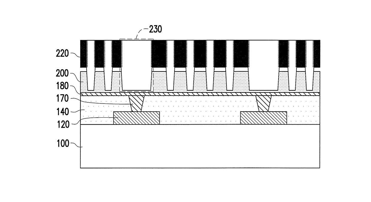
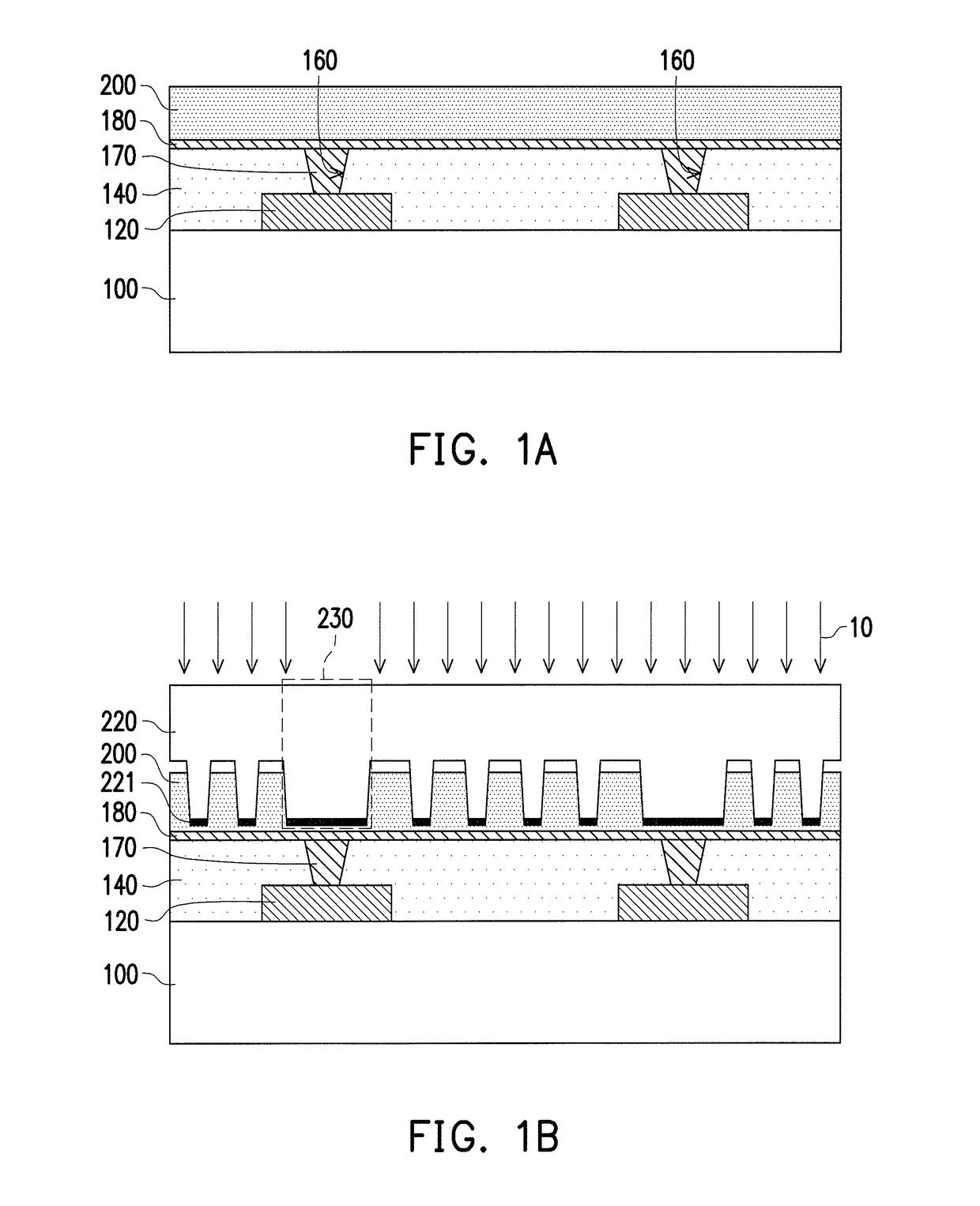
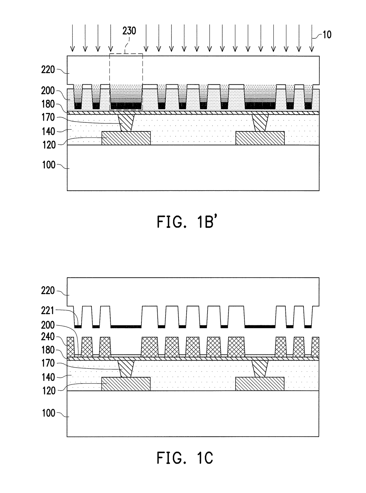
[0020]FIG. 1A to FIG. 1F are schematics of the manufacturing method of a circuit board according to the invention.

[0021]Referring to FIG. 1A, a circuit pattern 120 is formed on a dielectric substrate 100. The circuit pattern 120 is formed by, for instance, first forming a conductive layer on the dielectric substrate 100 via a lamination method and performing a patterning process on the conductive layer. The material of the dielectric substrate 100 is, for instance, epoxy resin, glass fiber cloth, or ceramic. The material of the circuit pattern 120 is, for instance, copper.

[0022]Next, a dielectric layer 140 is formed on the dielectric substrate 100 and covers the circuit pattern 120 on the dielectric substrate 100. The material of the dielectric layer 140 is, for instance, epoxy resin. The dielectric layer 140 is, for instance, formed on the dielectric substrate 100 via a lamination method. The dielectric layer 140 has a hole 160 exposing a portion of the circuit pattern 120. The for...

second embodiment

[0035]FIG. 2A to FIG. 2B are schematics of the manufacturing method of a circuit board according to the invention.

[0036]Referring to FIG. 2A, a circuit pattern 120 is formed on a dielectric substrate 100. Next, a dielectric layer 140 is formed on the dielectric substrate 100 and covers the circuit pattern 120 on the dielectric substrate 100, wherein the dielectric layer 140 has a hole 160 exposing a portion of the circuit pattern. Next, a conductive seed layer 420 is formed in the hole 160 and on the dielectric layer 140. In the present embodiment, the conductive seed layer 420 is formed on the side surface and the bottom surface of the hole 160. Next, the photoresist layer 200 is formed on the conductive seed layer 420 and the hole 160 is completely filled.

[0037]Then, referring to FIG. 2B, the manufacturing steps of FIG. 1B to FIG. 1F are performed to form a circuit pattern 460 (formed by a patterned metal layer 440 and the conductive seed layer 420 located on the dielectric layer ...

third embodiment

[0038]FIG. 3A to FIG. 3E are schematics of the manufacturing method of a circuit board according to the invention. In the present embodiment, the pressing side of the piezochromic stamp includes a portion of the piezochromic stamp and a piezochromic material layer attached to the portion. However, in another embodiment, the piezochromic stamp itself can also be made by a piezochromic material.

[0039]Referring to FIG. 3A, a circuit pattern 120 is formed on a dielectric substrate 100, wherein the circuit pattern 120 can be formed on a first surface 100a and a second surface 100b of the dielectric substrate 100. The circuit pattern 120 is formed by, for instance, first forming a conductive layer on the dielectric substrate 100 via a lamination method and performing a patterning process on the conductive layer. The material of the dielectric substrate 100 is, for instance, epoxy resin, glass fiber cloth, or ceramic. The material of the circuit pattern 120 is, for instance, copper.

[0040]N...


PUM

PropertyMeasurementUnit
conductiveaaaaaaaaaa
light transmittanceaaaaaaaaaa
specific wavelengthaaaaaaaaaa

Abstract

A manufacturing method of a circuit board and a piezochromic stamp are provided. A circuit pattern is formed on a dielectric substrate. A dielectric layer having a hole or a conductive via and covering the circuit pattern is formed on the dielectric substrate. A conductive seed layer is formed on the dielectric layer. A photoresist layer is formed on the conductive seed layer. A piezochromic stamp is imprinted on the photoresist layer, wherein when the pressing side of the piezochromic stamp is in contact with the conductive seed layer, the light transmittance effect thereof is changed to blocking or allowing light having a specific wavelength to pass through. A patterned photoresist layer is formed by using the piezochromic stamp as a mask. A patterned metal layer is formed on the exposed conductive seed layer. The patterned photoresist layer and the conductive seed layer are removed.

Description

CROSS-REFERENCE TO RELATED APPLICATION[0001]This application claims the priority benefit of U.S. provisional application Ser. No. 62 / 309,930, filed on Mar. 17, 2016. The entirety of the above-mentioned patent application is hereby incorporated by reference herein and made a part of this specification.BACKGROUND OF THE INVENTION[0002]Field of the Invention[0003]The invention relates to a manufacturing method of a circuit board and a stamp, and more particularly, to a piezochromic stamp and a manufacturing method of a circuit board formed by the piezochromic stamp.[0004]Description of Related Art[0005]Nano-imprint lithography (NIL) is a technique for manufacturing fine circuits and is extensively applied in the LED and OLED industries. NIL includes pressing a mold prototype having a pattern (generally referred to as mold, stamp, or template) on an etchant or a photoresist to mechanically deform the mold prototype so as to precisely transfer a fine pattern. Therefore, once the manufact...

Claims


Application Information

Patent Timeline
Patent Type & Authority Applications(United States)
IPC IPC(8): H05K3/06H05K3/10
CPCH05K3/06H05K2203/0502H05K3/108G03F7/0002H05K3/465Y10T29/49124Y10T29/49155H05K3/4644H05K2203/0108Y10T29/5313G03F7/162G03F7/20H05K1/115H05K3/064H05K2201/091H05K2203/0548H05K3/0023H05K2203/0369H05K2203/0562
Inventor CHENG, SHIH-LIAN
Owner UNIMICRON TECH CORP
Why Eureka
Try Eureka