Semiconductor Device, Electronic Component, and Electronic Device

a technology of semiconductor devices and components, applied in logic circuits, power consumption reduction, pulse techniques, etc., can solve problems such as increased power consumption, data generated that is not intended by a user, and data transfer between before and after context switches cannot be performed correctly, so as to suppress the influence of parasitic capacitance on circuit operation, suppress the generation of shoot-through current, and reduce parasitic capacitance

Inactive Publication Date: 2017-10-05
SEMICON ENERGY LAB CO LTD
View PDF1 Cites 7 Cited by
  • Summary
  • Abstract
  • Description
  • Claims
  • Application Information

AI Technical Summary

Benefits of technology

[0010]An object of one embodiment of the present invention is to provide a semiconductor device in which data transfer between before and after context switch can be performed correctly even at high clock frequency. Another object of one embodiment of the present invention is to provide a semiconductor device in which generation of shoot-through current can be suppressed.
[0011]Another object of one embodiment of the present invention is to provide a semiconductor device that is capable of reducing parasitic capacitance by suppressing influence of skew on circuit operation and reducing layout area for a skew countermeasure circuit and wiring routing.
[0012]Another object of one embodiment of the present invention is to provide a semiconductor device that is capable of equalizing time required for context signal switch with time required for store and load operations in the case where data of a flip-flop in a PLD is backed up.
[0019]According to one embodiment of the present invention, a semiconductor device in which data transfer between before and after context switch can be performed correctly even at high clock frequency can be provided. Alternatively, according to one embodiment of the present invention, a semiconductor device in which generation of shoot-through current can be suppressed can be provided.
[0020]Alternatively, according to one embodiment of the present invention, a semiconductor device that is capable of reducing parasitic capacitance by suppressing influence of skew on circuit operation and reducing layout area for a skew countermeasure circuit and wiring routing can be provided.

Problems solved by technology

As a result, data that is not intended by a user is generated, and data transfer between before and after the context switch cannot be performed correctly.
Furthermore, in the case of an incomplete circuit in which a high-potential output signal and a low-potential output signal are supplied to the same node, shoot-through current might be generated, which leads to an increase in power consumption.
In addition, in the case where data of the flip-flop in the PLD is backed up in accordance with context signal switch, if time required for store operation (operation of storing data from the flip-flop to a backup circuit) is different from time required for load operation (operation of restoring the data from the backup circuit to the flip-flop), it might be difficult to equalize time required for context signal switch and time required for store and load operations.

Method used


Image

  • Semiconductor Device, Electronic Component, and Electronic Device
  • Semiconductor Device, Electronic Component, and Electronic Device
  • Semiconductor Device, Electronic Component, and Electronic Device

Examples


embodiment 1

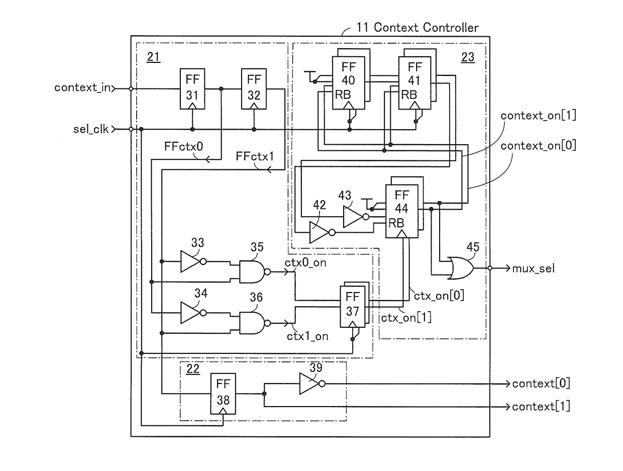
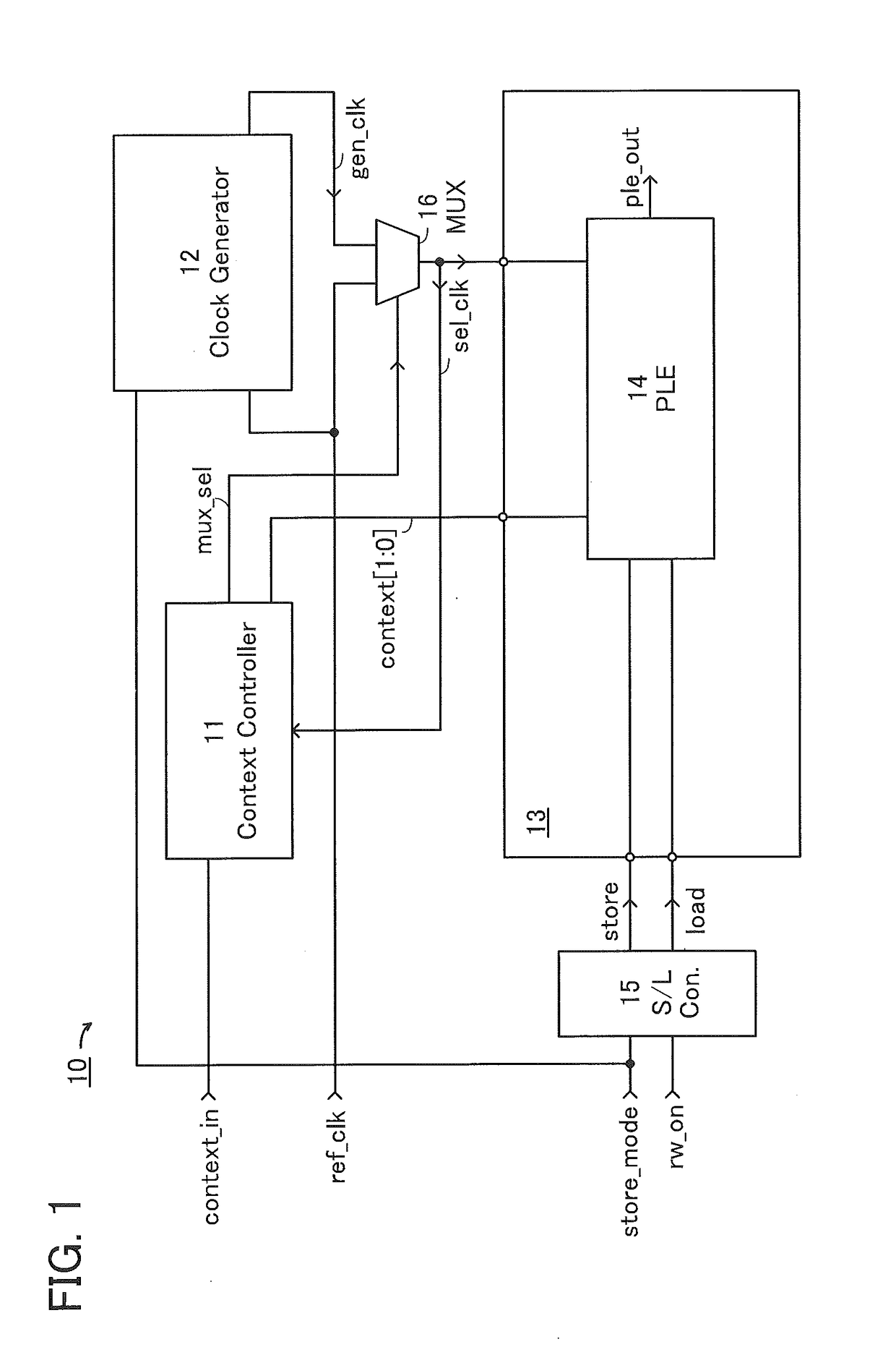
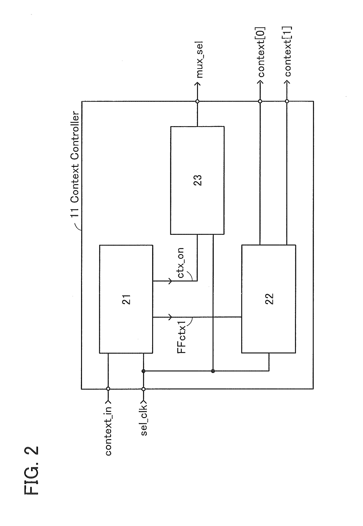
[0045]The structure and operation of a semiconductor device in one embodiment of the present invention are described with reference to FIG. 1, FIG. 2, FIG. 3, FIG. 4, FIG. 5, FIG. 6, FIG. 7, FIG. 8, FIG. 9, FIGS. 10A and 10B, FIGS. 11A and 11B, FIG. 12, and FIG. 13. Note that the semiconductor device in one embodiment of the present invention functions as a multi-context programmable logic device.

[0046]A semiconductor device 10 illustrated in a block diagram of FIG. 1 includes a context controller 11 (denoted by “Context Controller” in the diagram), a clock generation circuit 12 (denoted by “Clock Generator” in the diagram), and a programmable circuit 13. The semiconductor device 10 includes a store / load controller 15 (denoted by “S / L Con.” in the diagram) and a switch circuit 16 (denoted by “MUX” in the diagram) as other components. The programmable circuit 13 includes a programmable logic element 14 (denoted by “PLE” in the diagram and hereinafter referred to as “PLE 14”).

[0047]Th...

embodiment 2

[0177]In this embodiment, an example of a display system including the semiconductor device and an example of a display device applicable to a display device included in the display system are described.

[0178]FIG. 14 is a block diagram illustrating a structure example of a display system.

[0179]A display system 500 includes a video data communication portion 510, a display driver portion 520, a power source control portion 530, a display device portion 540, and a touch panel portion 550.

[0180]The video data communication portion 510 includes a wireless signal reception portion 511, a processor 512, and a video data input portion 513. The wireless signal reception portion 511 has a function of being connected to a wireless local area network (LAN) to receive video data or the like. The processor 512 decodes video data or the like received in the wireless signal reception portion 511 and outputs the decoded video data or the like to the display driver portion 520. The video data input ...

embodiment 3

[0226]In this embodiment, an IC chip, an electronic component, electronic devices, and the like are described as examples of a semiconductor device.

[0227]FIG. 17A is a flow chart showing an example of a method for manufacturing an electronic component. The electronic component is also referred to as a semiconductor package or an IC package. This electronic component has a plurality of standards and names depending on a terminal extraction direction and a terminal shape. Examples of the electronic component are described in this embodiment.

[0228]A semiconductor device including a transistor is completed by integrating detachable components on a printed wiring board through an assembly process (post-process). The post-process can be finished through steps in FIG. 17A. Specifically, after an element substrate obtained in a wafer process is completed (step ST71), a rear surface of the substrate is ground. The substrate is thinned in this step to reduce warpage or the like of the substra...


PUM


Abstract

Skew of a multi-context PLD in context switch is reduced to achieve low power consumption. The frequency of a clock signal is switched in context switch operation in accordance with circuit operation to secure time required for context switch. By returning the frequency of the clock signal to the original frequency after executing the context switch, the PLD can maintain high-speed processing and perform the context switch accurately and safely. The time required for the context switch mainly depends on a hardware structure (circuit layout including a parasitic component). Thus, the reliability in the context switch can be improved when time that is equal to or longer than the longest time required for circuit change is secured.

Description

BACKGROUND OF THE INVENTION1. Field of the Invention[0001]One embodiment of the present invention relates to a semiconductor device, an electronic component, and an electronic device.[0002]Note that one embodiment of the present invention is not limited to the above technical field. The technical field of the invention disclosed in this specification and the like relates to an object, a method, or a manufacturing method. Another embodiment of the present invention relates to a process, a machine, manufacture, or a composition of matter.[0003]In this specification and the like, a semiconductor device generally means a device that can function by utilizing semiconductor characteristics. A display device (e.g., a liquid crystal display device or a light-emitting display device), a projection device, a lighting device, an electrooptic device, a power storage device, a memory device, a semiconductor circuit, an imaging device, an electronic device, or the like includes a semiconductor de...

Claims


Application Information

Patent Timeline
Patent Type & Authority Applications(United States)
IPC IPC(8): H03K19/00H03K21/02H03K19/177
CPCH03K19/0008H03K19/17744H03K21/026H03K19/1776H03K19/17728
Inventor KOZUMA, MUNEHIROKUROKAWA, YOSHIYUKI
Owner SEMICON ENERGY LAB CO LTD
Why Eureka
Try Eureka