Semiconductor device, electronic component, and electronic device

a semiconductor and electronic component technology, applied in the field of semiconductor devices, can solve problems such as increased power consumption, data generated by users that cannot be intended by users, and data transfer between before and after context switches cannot be performed normally, so as to achieve high reliability, suppress the generation of shoot-through current, and reduce power consumption.

Inactive Publication Date: 2017-05-18
SEMICON ENERGY LAB CO LTD
View PDF20 Cites 5 Cited by
  • Summary
  • Abstract
  • Description
  • Claims
  • Application Information

AI Technical Summary

Benefits of technology

[0019]One embodiment of the present invention can provide a semiconductor device in which data transfer between before and after context switch can be performed normally even at a high clock frequency, or a semiconductor device in which generation of shoot-through current can be suppressed.
[0020]One embodiment of the present invention can provide a semiconductor device that is suitable for high-speed operation, a highly reliable semiconductor device, a semiconductor device with reduced power consumption, a semiconductor device including a transistor with a low off-state current, or a semiconductor device that can be used in a wide temperature range.
[0021]One embodiment of the present invention can provide a novel semiconductor device, a novel electronic device, and the like.

Problems solved by technology

As a result, data not intended by a user is generated, in which case data transfer between before and after context switch cannot be performed normally.
Furthermore, in the case of an incomplete circuit in which a high-potential output signal and a low-potential output signal are supplied to the same node, shoot-through current might be generated, which leads to an increase in power consumption.

Method used


Image

  • Semiconductor device, electronic component, and electronic device
  • Semiconductor device, electronic component, and electronic device
  • Semiconductor device, electronic component, and electronic device

Examples


embodiment 1

[0053]In this embodiment, a semiconductor device of one embodiment of the present invention will be described with reference to drawings.

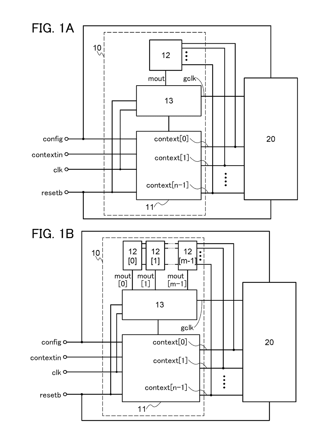
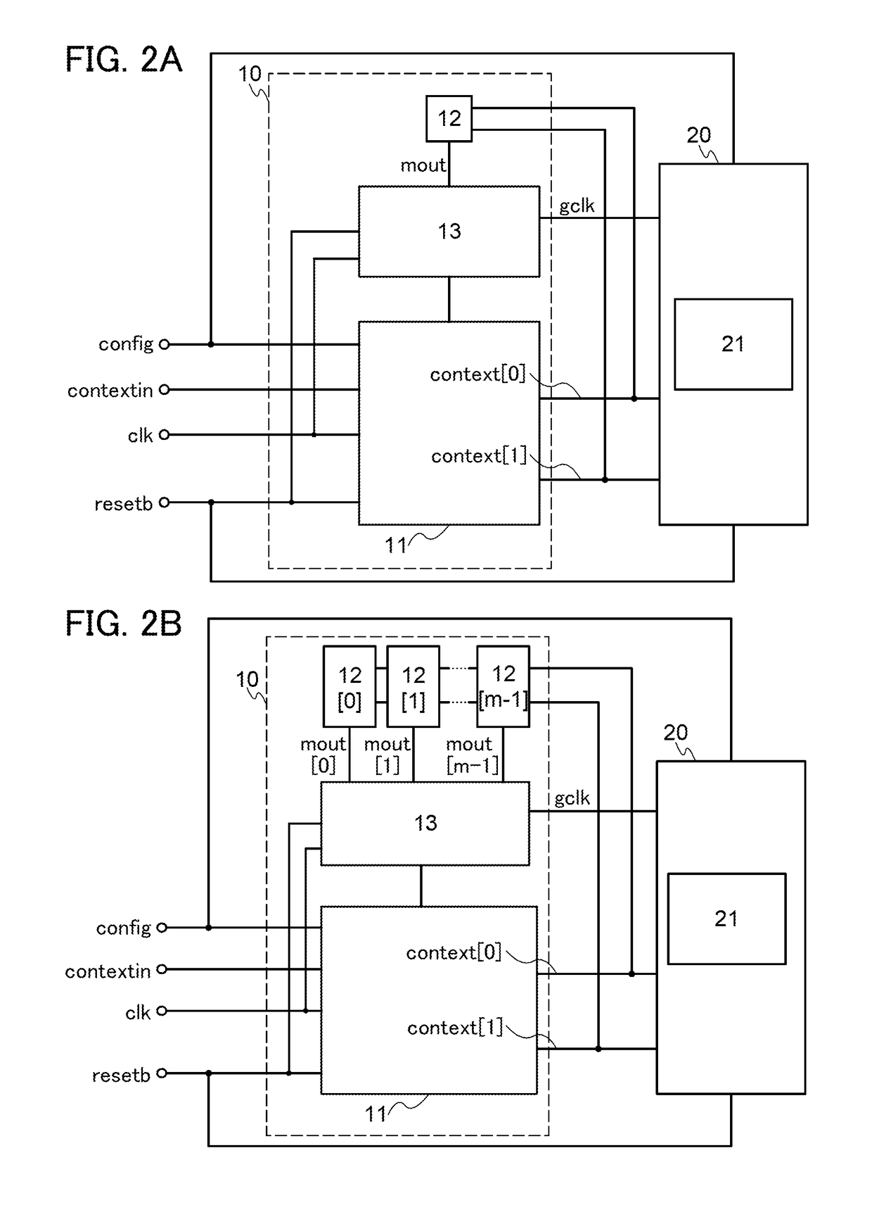
[0054]One embodiment of the present invention relates to a semiconductor device including a controller and a PLD controlled by the controller. The controller has a function of supplying a clock signal to the PLD. The reconfiguration of the PLD, or the like, is performed on the basis of the clock signal. Note that when a clock signal is input to the PLD during the reconfiguration of the PLD, or the like, abnormal data might be captured by the PLD, for example, leading to malfunction of the semiconductor device of one embodiment of the present invention. The semiconductor device of one embodiment of the present invention performs clock gating so that a clock signal can be prevented from being input to the PLD during reconfiguration or the like. Accordingly, the semiconductor device of one embodiment of the present invention can operate normally and o...

operation example

[0151]An operation example of the semiconductor device having the configuration illustrated in FIG. 2A will be described using a timing chart in FIG. 13A, and an operation example of the semiconductor device having the configuration illustrated in FIG. 2B will be described using a timing chart in FIG. 13B.

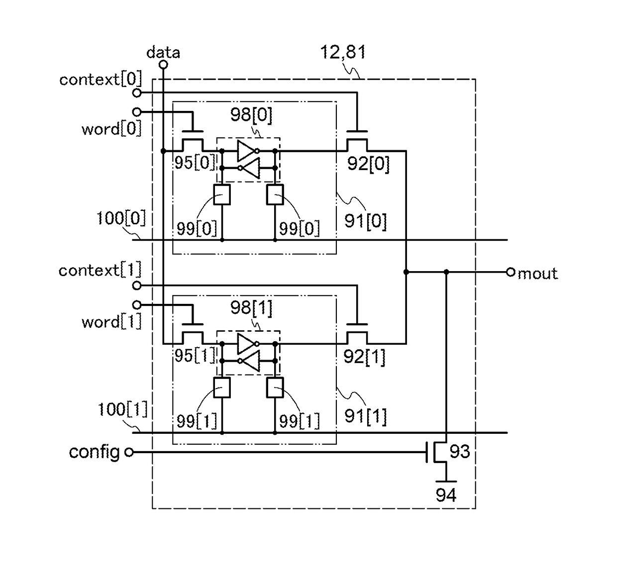
[0152]The timing charts in FIGS. 13A and 13B show the potentials of the signal clk, the signal resetb, the signal config, the signal contextin, the signal mout, the signal context[0], the signal context[1], and the signal gclk, and the configuration state of the PLD 20.

[0153]When the potential of the signal context[0] is at an H level, the configuration of the PLD 20 corresponds to configuration data retained in the memory cell 91[0] included in the configuration memory 81 or the like, for example. The PLD 20 with such a configuration is represented by “PLD 20_0.” When the potential of the signal context[1] is at an H level, the configuration of the PLD 20 corresponds to configurat...

embodiment 2

[0178]In this embodiment, an electronic component, an imaging device, an electronic device including an electronic component, and the like will be described as examples of semiconductor devices.

[0179]FIG. 14A is a flow chart showing an example of a method for manufacturing an electronic component. An electronic component is also referred to as a semiconductor package, an IC package, or a package. For the electronic component, there are various standards and names corresponding to the direction or the shape of terminals; hence, one example of the electronic component will be described in this embodiment.

[0180]A semiconductor device including a transistor is completed by integrating detachable components on a printed circuit board through the assembly process (post-process). The post-process can be completed through steps shown in FIG. 14A. Specifically, after an element substrate is completed in a wafer process (51), a dicing step for dividing the substrate into a plurality of chips ...


PUM


Abstract

A semiconductor device includes a configuration memory that has functions of holding configuration data and generating a signal based on the configuration data, a context generator that has a function of generating a signal for controlling context switch, a clock generator that has a function of operating in a first mode or a second mode in accordance with the signal generated in the configuration memory, and a PLD. A clock signal is input to the context generator and the clock generator. The clock generator outputs the clock signal to the PLD in the first mode and stops outputting the clock signal to the PLD in the second mode.

Description

TECHNICAL FIELD[0001]One embodiment of the present invention relates to a semiconductor device.[0002]Note that one embodiment of the present invention is not limited to the above technical field. The technical field of one embodiment of the invention disclosed in this specification and the like relates to an object, a method, or a manufacturing method. One embodiment of the present invention relates to a process, a machine, manufacture, or a composition of matter. Specific examples of the technical field of one embodiment of the present invention disclosed in this specification and the like include a semiconductor device, a display device, a liquid crystal display device, a light-emitting device, a lighting device, a power storage device, a memory device, an imaging device, a method for operating any of them, and a method for manufacturing any of them.[0003]In this specification and the like, a semiconductor device generally means a device that can function by utilizing semiconducto...

Claims


Application Information

Patent Timeline
Patent Type & Authority Applications(United States)
IPC IPC(8): H03K19/177
CPCH03K19/17764H03K19/1774H03K19/1776H03K19/17728H03K19/17792
Inventor KOZUMA, MUNEHIRO
Owner SEMICON ENERGY LAB CO LTD
Why Eureka
Try Eureka