High electron mobility transistor (HEMT)

a high electron mobility, transistor technology, applied in the direction of semiconductor devices, semiconductor/solid-state device details, electrical apparatus, etc., can solve the problem and achieve the effect of increasing the breakdown voltage of the hemt and reducing the strength of the electric field

Active Publication Date: 2017-11-16
RFHIC
View PDF0 Cites 15 Cited by
  • Summary
  • Abstract
  • Description
  • Claims
  • Application Information

AI Technical Summary

Benefits of technology

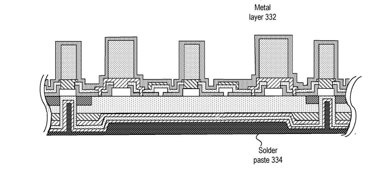
[0009]In embodiments, a drain field plate is formed over the drain of a HEMT. The drain field plate includes a metal pad that has a larger projection area than the drain pad.

Problems solved by technology

The drain field plate reduces the strength of the electric field that is generated by t

Method used


Image

  • High electron mobility transistor (HEMT)
  • High electron mobility transistor (HEMT)
  • High electron mobility transistor (HEMT)

Examples


Embodiment Construction

[0035]In the following description, for purposes of explanation, specific details are set forth in order to provide an understanding of the disclosure. It will be apparent, however, to one skilled in the art that the disclosure can be practiced without these details. Furthermore, one skilled in the art will recognize that embodiments of the present disclosure, described below, may be implemented in a variety of ways, such as a process, an apparatus, a system, a device, or a method on a tangible computer-readable medium.

[0036]One skilled in the art shall recognize: (1) that certain steps may optionally be performed; (2) that steps may not be limited to the specific order set forth herein; and (3) that certain steps may be performed in different orders, including being done contemporaneously.

[0037]Elements / components shown in diagrams are illustrative of exemplary embodiments of the disclosure and are meant to avoid obscuring the disclosure. Reference in the specification to “one embo...


PUM


Abstract

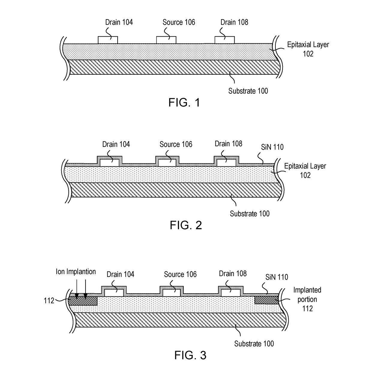
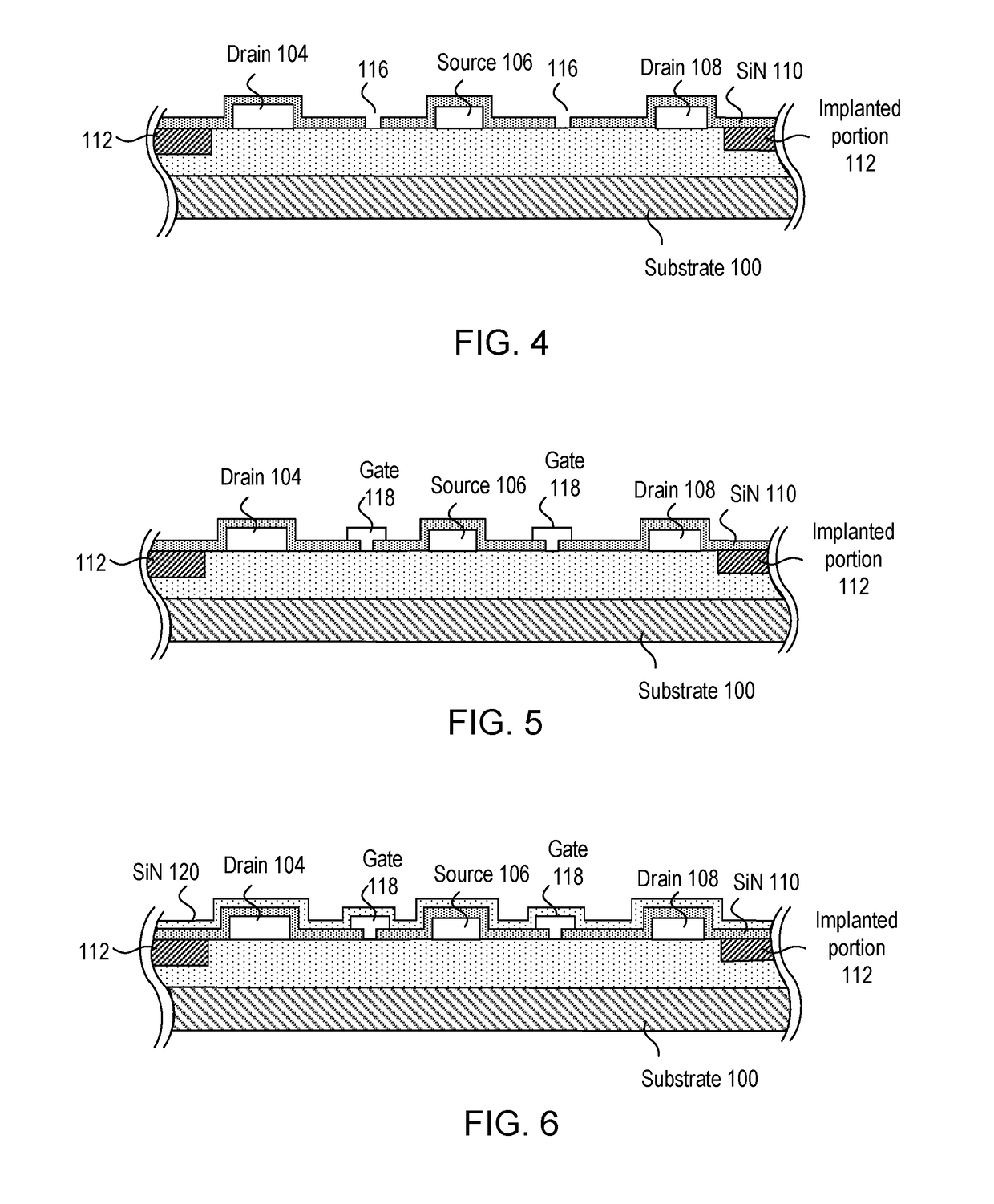
HEMT having a drain field plate is provided. The drain field plate is formed in the area between the gate and drain of a HEMT. The drain field plate includes a metal pad that has a larger projection area than the drain pad. The drain field plate and semiconductor layer disposed beneath the drain field plate form a metal-semiconductor (M-S) Schottky structure. The capacitance of the M-S Schottky structure generates capacitance in the semiconductor area, which increases the breakdown voltage of the transistor components of the HEMT. A portion of the substrate under the active area may be removed to thereby increase the heat conductivity and reduce the junction temperature of the transistor components of the HEMT.

Description

CROSS REFERENCE TO PRIOR APPLICATIONS[0001]This application claims priority to U.S. Provisional Patent Application No. 62 / 334,837, filed on May 11, 2016, which is hereby incorporated by reference in its entirety.BACKGROUND[0002]A. Technical Field[0003]The present invention relates to semiconductor devices, and more particularly, to high electron mobility transistors.[0004]B. Background of the Invention[0005]The high electron mobility transistor (HEMT), also known as heterostructure FET (HFET) or modulation-doped FET (MODFET), is a type of field effect transistor (FET) in which a hetero-junction between a channel layer and a barrier layer whose electron affinity is smaller than that of the channel layer is formed. HEMT transistors are able to operate at higher frequencies than ordinary transistors, up to millimeter wave frequencies, and are typically used in high-frequency and high-power products, such as power amplifier between mobile phone stations and phased array laser in militar...

Claims


Application Information

Patent Timeline
IPC IPC(8): H01L29/40H01L21/8252H01L23/48H01L29/778H01L23/00H01L21/768H01L29/205H01L29/20H01L27/06H01L29/66
CPCH01L29/404H01L29/2003H01L29/205H01L29/408H01L29/7787H01L29/401H01L29/66462H01L21/8252H01L21/76898H01L27/0605H01L23/481H01L24/29H01L2224/29025H01L2924/1033H01L2924/13064H01L29/7783H01L29/402H01L29/4175H01L29/7786H01L29/0619H01L29/0657H01L2224/29009H01L24/05H01L24/94H01L2224/04026H01L2224/0557H01L2224/05644H01L2224/83191H01L2224/94H01L2224/05583H01L2224/05572H01L2224/29022H01L2224/05027H01L2924/10344H01L24/03H01L2224/0345H01L2224/03462H01L2224/05073H01L2224/0508H01L2224/05084H01L2224/293H01L2224/29294H01L2224/05139H01L2224/05147H01L2224/32245H01L2224/05144H01L2224/05166H01L2224/03H01L2224/27H01L2924/00014H01L2924/014H01L2224/05639H01L29/452H01L27/085H01L21/8232H01L21/823481
Inventor LEE, WON SANG
Owner RFHIC
Why Eureka
Try Eureka