Check patentability & draft patents in minutes with Patsnap Eureka AI!

Three-Transistor OTP Memory Cell

a memory cell and three-transistor technology, applied in the field of three-transistor otp memory cells, can solve the problems of adversely affecting the post-programmed resistance and therefore the reading of the state of the quality of the programmed connection in the memory cell, so as to enhance the programmability of the memory cell and enhance the otp memory cell. programmability

Active Publication Date: 2017-12-14
SYNOPSYS INC
View PDF3 Cites 1 Cited by
  • Summary
  • Abstract
  • Description
  • Claims
  • Application Information

AI Technical Summary

Benefits of technology

The present invention provides an integrated circuit OTP memory cell that includes a programming MOSFET and two pass transistors. The two pass transistors, which are symmetrically located with respect to the programming MOSFET, enhance the programmability of the memory cell. One of the pass transistors is connected to the first conducting line and the other pass transistor is connected to the second conducting line. The programming MOSFET has a gate electrode that controls electrical connection between its two source / drain regions, which are connected to the first and second conducting lines, respectively. The method of programming the memory cell involves accessing the two source / drain regions, driving them to a first voltage, and driving the gate electrode to a second voltage to create a high voltage differential between them. The programming of the OTP memory cell is improved.

Problems solved by technology

Even though OTP memory cell arrays have been in use for many years, a persistent problem is the variability in the quality of the programmed connection in a memory cell.
That is, physical variations in the OTP memory cells adversely affect the post-programmed resistance and therefore the reading of the OTP memory cell state.

Method used


Image

  • Three-Transistor OTP Memory Cell
  • Three-Transistor OTP Memory Cell
  • Three-Transistor OTP Memory Cell

Examples


Embodiment Construction

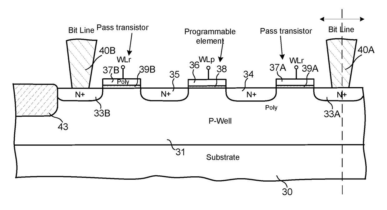
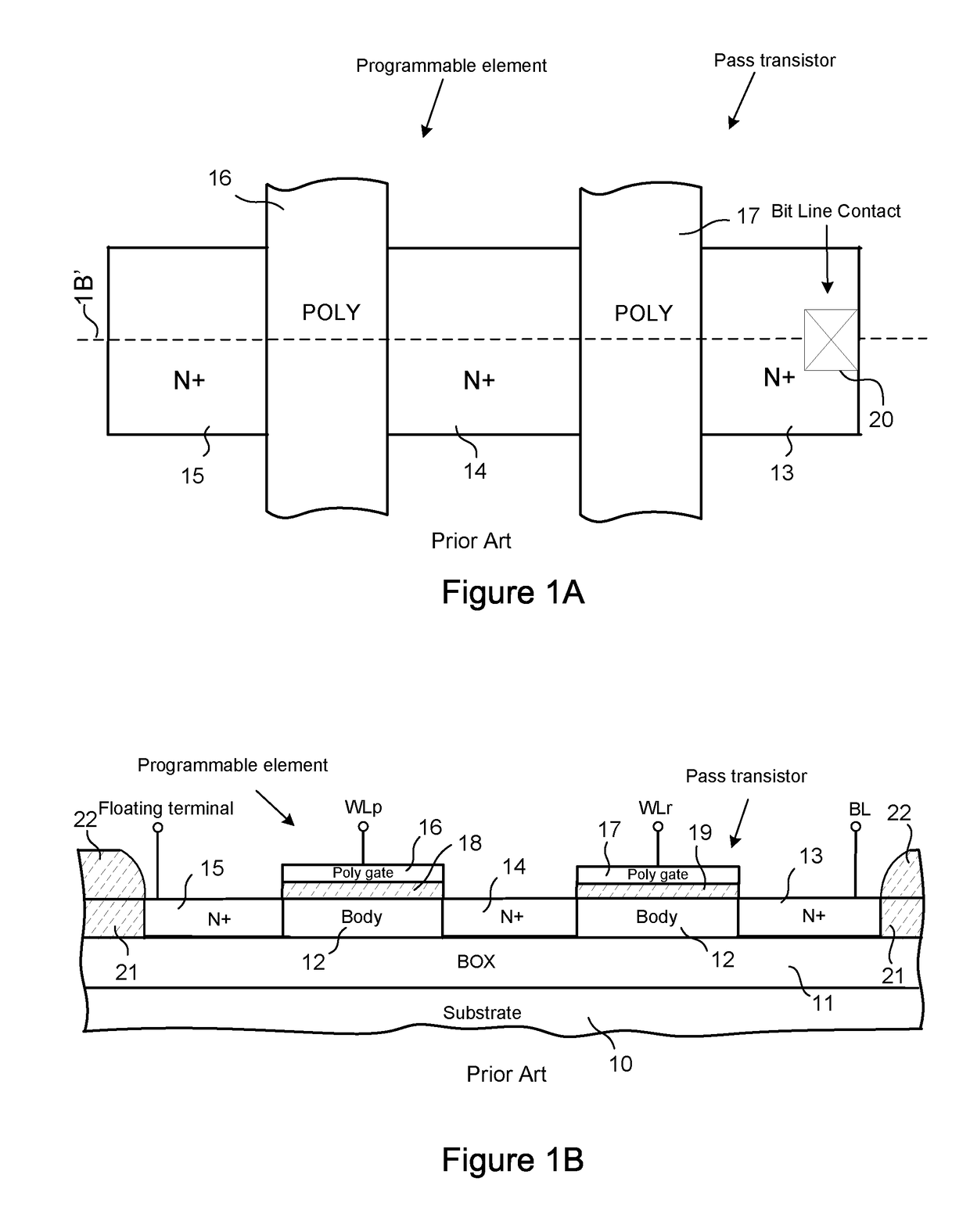
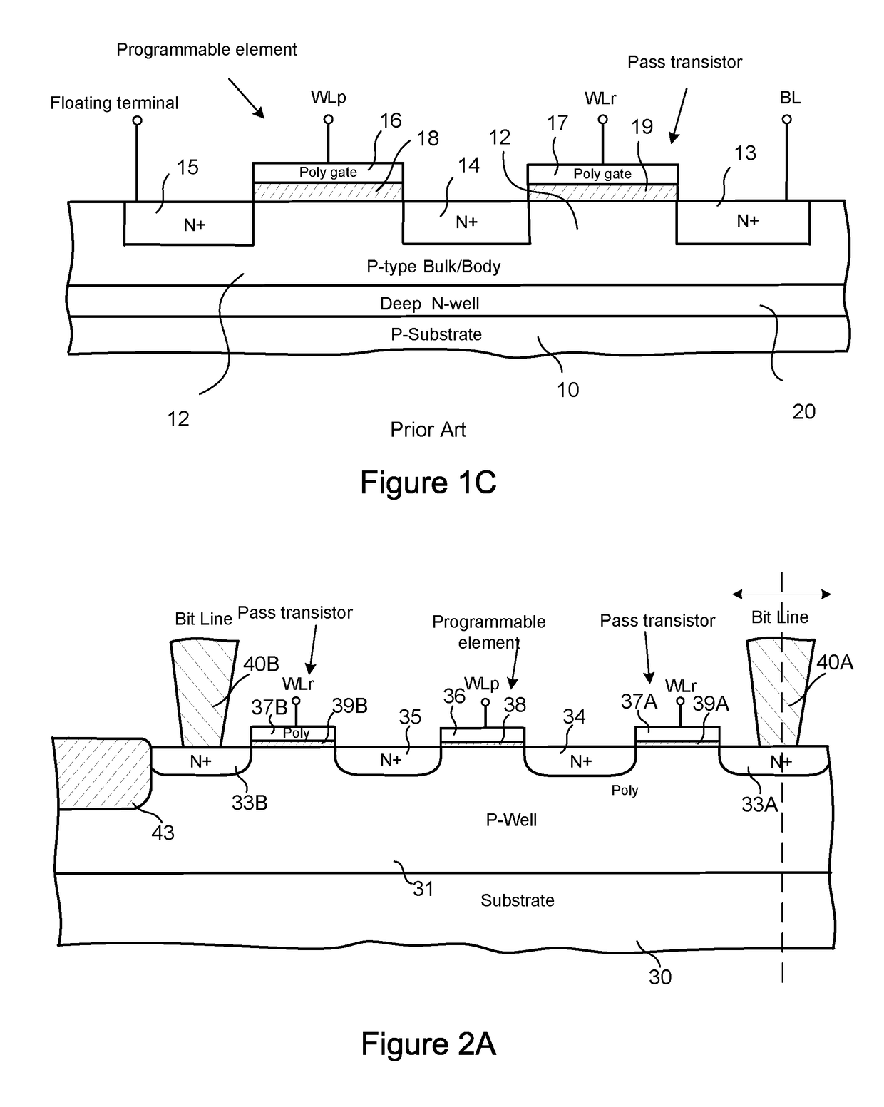
[0011]FIG. 1A is a top layout view of a current two-transistor OTP memory cell, which has a pass transistor and a programmable element, a second transistor. The two transistors are MOSFETs, each with a gate electrode over a channel region separating two source / drain regions. In the FIG. 1A memory cell the pass or select transistor is formed by a gate electrode 17 over a channel region which separates two N+ source / drain regions 13 and 14 located in a semiconductor body 12 of P-conductivity. A thin insulating oxide layer 19 (see FIG. 1B), called a gate oxide and not shown in this top view, separates the body 12 and N+ regions 13 and 14 from the gate electrode 17. The two source / drain regions 13 and 14 and the gate electrode 17 define a channel region on the top of the body 12 for the pass transistor. The N+ source / drain region 13 is connected to a bit line above (not shown) by a conducting plug 20.

[0012]Besides the pass transistor, the N+ source / drain region 14 also forms a source / dr...


PUM


Abstract

An OTP (One-Time Programmable) memory cell in an array has a programming MOSFET and symmetrically placed access transistors on either side of the programming MOSFET. The balanced layout of the memory cell improves photolithographic effects with a resulting improved process results. Results of programming the memory cell is also improved.

Description

CROSS-REFERENCE TO RELATED APPLICATIONS[0001]This patent application claims the benefit of U.S. Provisional Patent Application No. 62 / 348,732, filed Jun. 10, 2016, which is incorporated by reference along with all other references cited in this application.BACKGROUND OF THE INVENTION[0002]This invention relates to an improved OTP (One-Time Programmable) memory cell and, in particular, a three-transistor OTP memory cell with improved programmability.[0003]NVM (Nonvolatile memory) integrated circuits retain stored data even after power is removed. Such devices are found in many consumer electronics and industrial applications. A common memory cell in NVM integrated circuits is the antifuse memory cell based upon the programming of a gate dielectric layer. Such antifuse memory cells, more particularly, the one-time programmable (OTP) memory cell, are commonly used by integrated circuit designers since such cells are compatible with standard logic CMOS (Complementary Metal-Oxide-Semicon...

Claims


Application Information

Patent Timeline
Patent Type & Authority Applications(United States)
IPC IPC(8): G11C17/18H01L27/112H01L23/535G11C17/16
CPCG11C17/18G11C17/16H01L23/535H01L27/11206H10B20/25G11C17/14
Inventor LUAN, HARRYSU, TAOWANG, LARRYCHENG, CHARLIE
Owner SYNOPSYS INC
Features
  • R&D
  • Intellectual Property
  • Life Sciences
  • Materials
  • Tech Scout
  • Unparalleled Data Quality
  • Higher Quality Content
  • 60% Fewer Hallucinations
Learn More