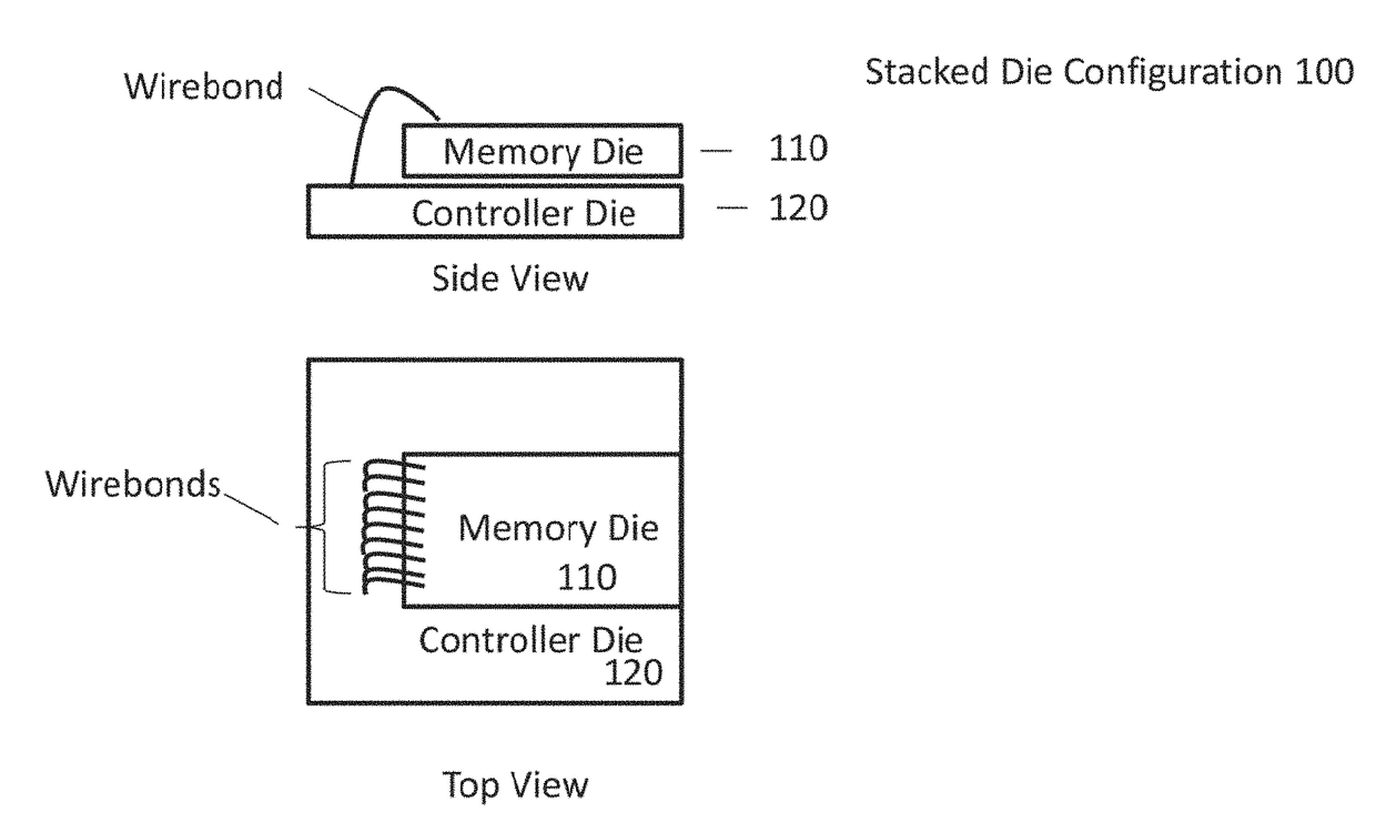
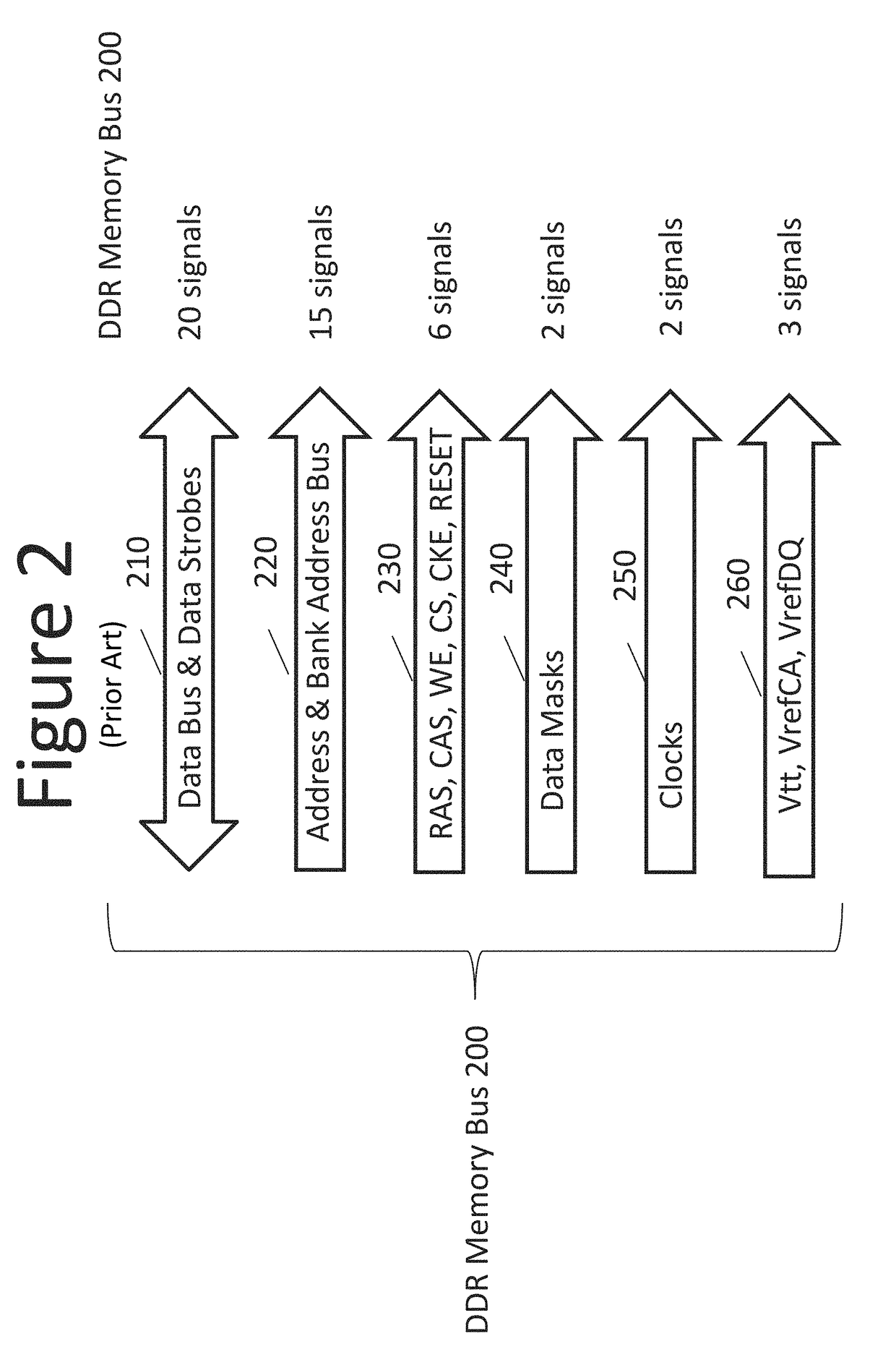
Low-pincount high-bandwidth memory and memory bus

a high-bandwidth memory and low-pincount technology, applied in the field of low-pincount high-bandwidth memory and memory bus, can solve the problems of limiting the performance of the memory bus, adding cost with little marginal benefit, and not being able to access multi-bank drams in burst read mod
US20170364469A1Active Publication Date: 2017-12-21ETRON TECH AMERICA INC

Patent Information

Authority / Receiving Office
US · United States
Patent Type
Applications(United States)
Current Assignee / Owner
ETRON TECH AMERICA INC
Publication Date
2017-12-21

Smart Images

  • Figure 1
    Figure 1
  • Figure 2
    Figure 2
  • Figure 3
    Figure 3
Patent Text Reader

Abstract

A memory subsystem is provided, including a memory controller integrated circuit (IC), a memory bus and a memory IC, all which use fewer signals than common DDR type memory of the same peak bandwidth. Using no more than 22 switching signals, the subsystem can transfer data over 3000 Megabytes / second across the bus interconnecting the ICs. Signal count reduction is attained by time-multiplexing address / control commands onto at least some of the same signals used for data transfer. A single bus signal is used to initiate bus operation, and once in operation the single signal can transfer addressing and control information to the memory IC concurrent with data transfer via a serial protocol based on 16 bit samples of this single bus signal. Bus bandwidth can be scaled by adding additional data and data strobe IO signals. These additional data bus signals might be used only for data and data mask transport. The physical layout of one version of the memory IC dispatches switching signal terminals adjacent to one short edge of the memory die to minimize the die area overhead for controller IC memory interface circuitry when used in a stacked die multi-chip package with said memory controller IC. The memory IC interface signal placement and signal count minimize signal length and circuitry for the memory bus signals.
Need to check novelty before this filing date? Find Prior Art

Description

CROSS-REFERENCE TO RELATED APPLICATIONS

[0001] The present application claims the benefit of the filing date of U.S. Provisional Patent Application No. 62 / 351,556 filed Jun. 17, 2016, the disclosure of which is hereby incorporated herein by reference.BACKGROUND OF THE INVENTIONTechnical Field

[0002] The present disclosure is directed to the area of buses and memory devices used in computing and data buffering applications such as execution memory or buffer memory and buses useful for communicating therewith.Description of the Related Art

[0003] High-bandwidth buffer memory and buses can be used in multiple applications including video applications that advantageously use a memory bus to connect memory to system logic.

[0004] Video Display Systems in portable devices may incorporate “Panel Self Refresh” buffer memory in the display panel to enable power savings when the information on the display is unchanging.

[0005] To improve image quality and to reduce flicker, large format display systems...

Claims
