Method for doping semiconductors

a semiconductor and semiconductor technology, applied in the field of doping semiconductors, can solve the problems of not having major industrial importance, not using the etching technique in industrial practice, and not completely suppressing the diffusion on the back, so as to improve the light yield, improve the effect of efficiency and improve the properties

Inactive Publication Date: 2017-12-28
MERCK PATENT GMBH
View PDF2 Cites 2 Cited by
  • Summary
  • Abstract
  • Description
  • Claims
  • Application Information

AI Technical Summary

Benefits of technology

[0070]In particular, however, the present invention also relates to the solar cells and photovoltaic elements produced by these process steps, which, owing to the process described here, have significantly improved properties, such as better light yield and thus improved efficiency, i.e. higher current yield.

Problems solved by technology

However, this etching technique is hardly still used in industrial practice.
Further gas mixtures are conceivable, but currently do not have major importance industrially.
The latter variant enables predominantly single-sided doping, but does not completely suppress diffusion on the back.
As a consequence of this, the front and back of the solar cell will have been short-circuited via a parasitic and residue p-n junction (tunnel contact), which reduces the conversion efficiency of the later solar cell.
However, this is only one of many different possibilities for the production of the desired metal contacts.
The choice of alternative doping technologies, as an alternative to the gas-phase doping already described in the introduction, is generally also unable to solve the problem of the production of regions with locally different doping on the silicon substrate.
However, it is disadvantageous in this process that in each case only one polarity (n or p) of the doping can be achieved.
This process enables expensive structuring steps to be saved.
Nevertheless, the disadvantage of possibly desired simultaneous doping of two polarities on the same surface at the same time (co-diffusion) cannot be compensated for, since this process is likewise based on pre-deposition of a dopant source which is only activated subsequently for the release of the dopant.
A disadvantage of this (post)doping from such sources is the unavoidable laser damage of the substrate: the laser beam must be converted into heat by absorption of the radiation.
However, the overall process is in reality accompanied by the formation of laser radiation-induced defects, which may be attributable to incomplete epitactic solidification and thus the formation of crystal defects.
A further disadvantage of laser beam-supported diffusion is the relative inefficiency if relatively large areas are to be doped quickly, since the laser system scans the surface in a dot-grid process.
This disadvantage naturally has less weight in the case of narrow regions to be doped.
However, laser doping requires sequential deposition of the post-treatable glasses.

Method used


Image

  • Method for doping semiconductors
  • Method for doping semiconductors
  • Method for doping semiconductors

Examples


example 1

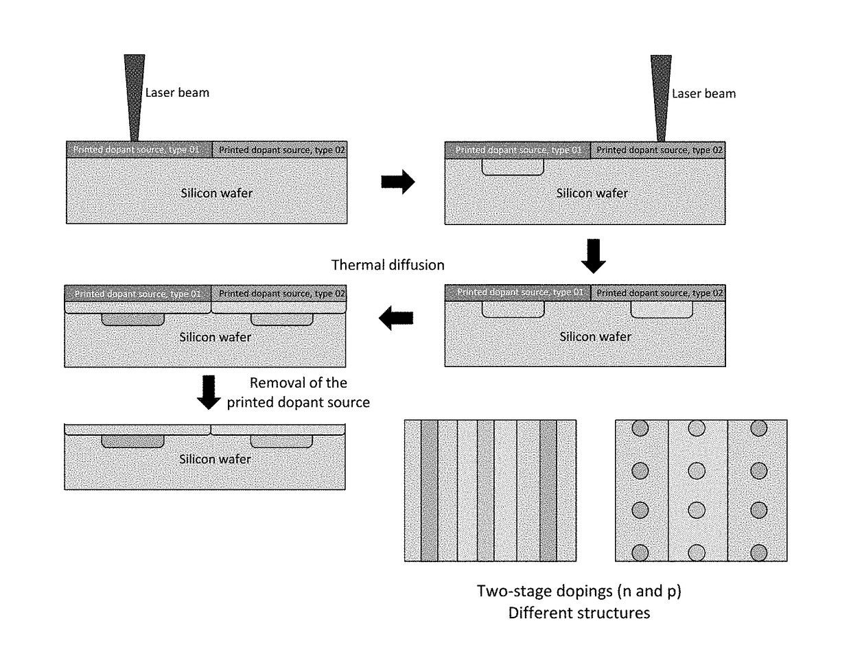
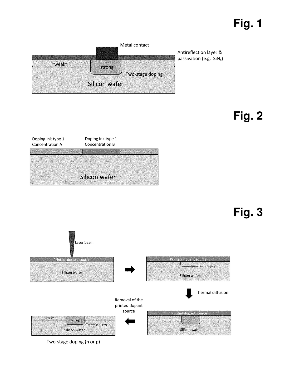
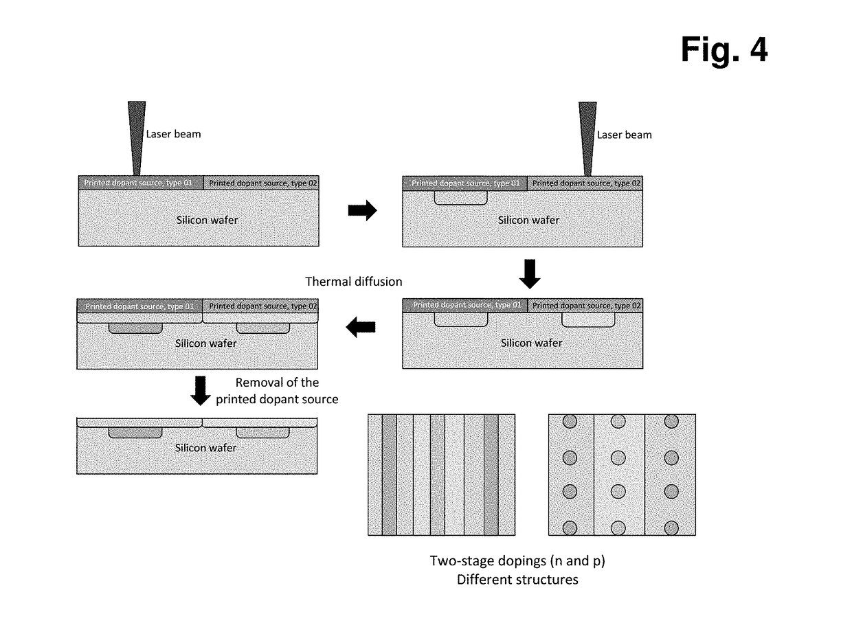
[0136]A textured 6″ CZ wafer with phosphorus base doping, having a resistivity of 2 ohm*cm, is printed with a boron doping paste, as described in the patent applications WO 2012 / 119686 A1 and WO 2014 / 101989 A1, using a steel screen (mounting angle)22.5° having a wire diameter 25 μm and an emulsion thickness of 10 μm using a doctor-blade speed of 110 mm / s, a doctor-blade pressure of 1 bar and a printing screen separation of 1 mm, where, depending on the other printing parameters, a layer thickness between 100 nm and 400 nm becomes established after complete drying at 600° C. After printing, the printed-on paste is dried for three minutes at 300° C. on a conventional laboratory hotplate. The wafer is then treated in predefined fields with the aid of an Nd:YAG nanosecond laser having a wavelength of 532 nm and using various laser fluences acting on the dried-on dopant source. The dopings of the various fields on the wafer are subsequently determined with the aid of four-point measureme...


PUM


Abstract

The present invention relates to a process for the production of structured, highly efficient solar cells and of photovoltaic elements which have regions of different doping. The invention likewise relates to the solar cells having increased efficiency produced in this way.

Description

[0001]The present invention relates to a process and composition for the production of structured, highly efficient solar cells and of photovoltaic elements which have regions of different doping. The invention likewise relates to the solar cells having increased efficiency produced in this way.PRIOR ART[0002]The production of simple solar cells or the solar cells which are currently represented with the greatest market share in the market comprises the essential production steps outlined below:[0003]1) Saw-damage etching and texture[0004]A silicon wafer (monocrystalline, multicrystalline or quasi-monocrystalline, base doping p or n type) is freed from adherent saw damage by means of etching methods and “simultaneously” textured, generally in the same etching bath. Texturing is in this case taken to mean the creation of a preferentially aligned surface nature as a consequence of the etching step or simply the intentional, but not particularly aligned roughening of the wafer surface....

Claims


Application Information

Patent Timeline
Patent Type & Authority Applications(United States)
IPC IPC(8): H01L21/22H01L31/18H01L31/0288
CPCH01L21/2225H01L31/0288H01L31/1804Y02E10/547Y02P70/50H01L31/186H01L31/02167
Inventor DOLL, OLIVERKOEHLER, INGOBARTH, SEBASTIAN
Owner MERCK PATENT GMBH
Why Eureka
Try Eureka