Indium electroplating compositions and methods for electroplating indium

a technology of indium electroplating and composition, applied in the direction of basic electric elements, semiconductor devices, etc., can solve the problems of increasing surface roughness, difficult reproducibility of plate void-free uniform indium of target thickness and smooth surface morphology on metal layers, corrosion of indium in galvanic interaction, etc., to reduce damage on assembled chips

Inactive Publication Date: 2018-01-18
ROHM & HAAS ELECTRONICS MATERIALS LLC
View PDF1 Cites 2 Cited by
  • Summary
  • Abstract
  • Description
  • Claims
  • Application Information

AI Technical Summary

Benefits of technology

The invention provides electroplating compositions that can produce void-free, uniform indium deposits with smooth surface morphology. This allows for the expanded use of indium in the electronics industry, including in semiconductors and thin film solar cells. The indium deposits can also be used as low temperature solder materials and thermal interface materials to protect electronic devices. This invention solves the problem of previous inability to electroplate indium with the required properties for advanced electronic applications.

Problems solved by technology

The ability to reproducibly plate void-free uniform indium of target thickness and smooth surface morphology on metal layers is challenging.
Indium reduction occurs at potentials more negative than that of proton reduction, and significant hydrogen bubbling at the cathode causes increased surface roughness.
In the absence of a complexing agent, indium ions begin to precipitate from solutions above pH>3. Plating indium on metals such as nickel, tin, copper and gold is challenging because these metals are good catalysts for proton reduction and are more noble than indium, thus they can cause corrosion of indium in a galvanic interaction.
Indium may also form undesired intermetallic compounds with these metals.
Finally, indium chemistry and electrochemistry have not been well studied, thus interactions with compounds that may serve as additives are unknown.
In general, conventional indium electroplating baths have not been able to electroplate an indium deposit which is compatible with multiple under bump metals (UBM) such as nickel, copper, gold and tin.
More importantly, conventional indium electroplating baths have not been able to electroplate indium with high coplanarity and high surface planarity on substrates which include nickel.
Although the foregoing TIMs have been adequate for many semiconductor devices, the increased performance of semiconductor devices has rendered such TIMs inadequate.

Method used


Image

  • Indium electroplating compositions and methods for electroplating indium
  • Indium electroplating compositions and methods for electroplating indium
  • Indium electroplating compositions and methods for electroplating indium

Examples


example 2

[0054]The method described in Example 1 above was repeated except that the indium electroplating composition included the following components:

TABLE 2COMPONENTAMOUNTIndium sulfate45g / LCitric acid96g / LSodium citrate dihydrate59g / LGuanylthiourea0.75g / L

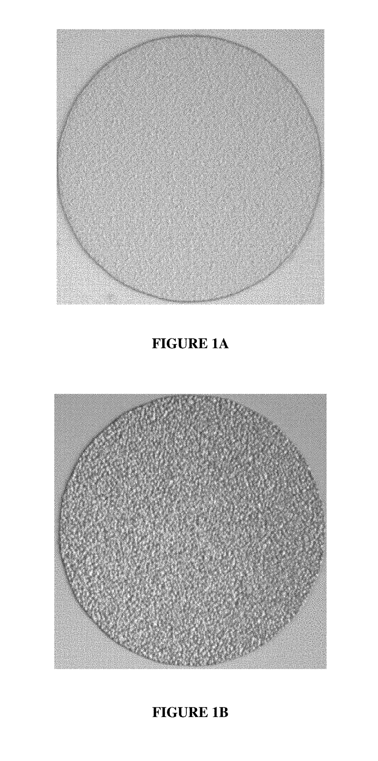
[0055]The nickel plated silicon wafers were immersed in the indium electroplating composition and indium metal was electroplated on the nickel. Indium electroplating was done at 25° C. at a current density of 4ASD for 30 seconds. The pH of the composition was 2.4. The anode was an indium soluble electrode. After indium was electroplated on the nickel layers, the photoresist was stripped from the wafers and the indium morphology was observed. All of the indium deposits appeared uniform and smooth.

[0056]FIG. 2 is an optical microscope image of one of the indium metal deposits electroplated on the nickel layer. The indium deposit appeared smooth in contrast to the indium deposit of FIG. 1B.

example 3

[0057]The method described in Example 1 above was repeated except that the indium electroplating composition included the following components:

TABLE 3COMPONENTAMOUNTIndium sulfate45g / LCitric acid96g / LSodium citrate dihydrate59g / LTetramethyl-2-thiourea0.5g / L

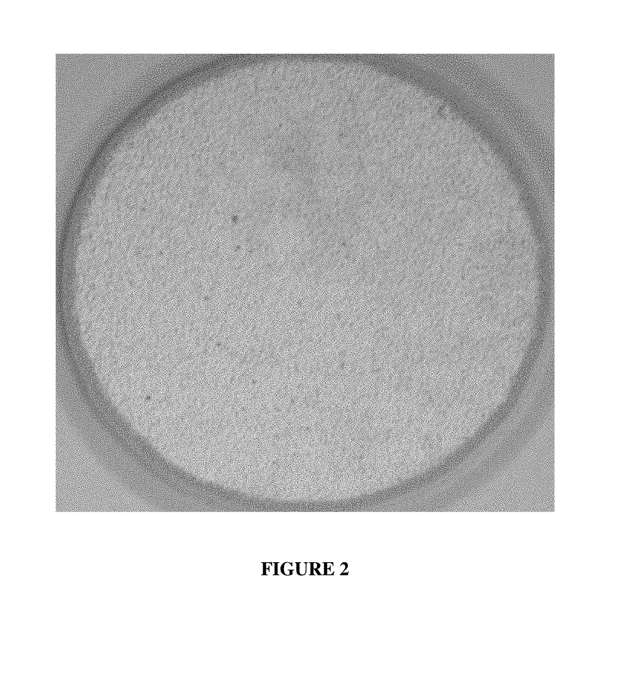
[0058]The nickel plated silicon wafers were immersed in the indium electroplating composition and indium metal was electroplated on the nickel. Indium electroplating was done at 25° C. at a current density of 4ASD for 30 seconds. The pH of the composition was 2.4. After indium was electroplated on the nickel, the photoresist was stripped from the wafers and the indium morphology was observed. All of the indium deposits appeared uniform and smooth.

[0059]FIG. 3 is an optical microscope image of one of the indium metal deposits electroplated on the nickel. The indium deposit appeared smooth in contrast to the indium deposit of FIG. 1B.

example 4

[0060]The method described in Example 1 above was repeated except that the silicon wafers were patterned with photoresist to have rectangular vias having lengths of 50 μm and the indium electroplating composition included the following components:

TABLE 4COMPONENTAMOUNTIndium sulfate45g / LCitric acid96g / LSodium citrate dihydrate59g / L1-allyl-2-thiourea11g / L1synonym = N-allyl-thiourea

[0061]The nickel plated silicon wafers were immersed in the indium electroplating composition and indium metal was electroplated on the nickel. Indium electroplating was done at 25° C. at a current density of 4ASD for 11 seconds. The pH of the composition was 2.4. After indium was electroplated on the nickel, the photoresist was stripped from the wafers and the indium morphology was observed. All of the indium deposits appeared uniform and smooth.

[0062]FIG. 4 is an optical microscope image of one of the indium metal deposits electroplated on the nickel layer. The indium deposit appeared smooth in contrast t...


PUM

PropertyMeasurementUnit
Thicknessaaaaaaaaaa
Thicknessaaaaaaaaaa
Densityaaaaaaaaaa

Abstract

Indium electroplating compositions electroplate substantially defect-free uniform layers which have a smooth surface morphology on metal layers. The indium electroplating compositions can be used to electroplate indium metal on metal layers of various substrates such as semiconductor wafers and as thermal interface materials.

Description

FIELD OF THE INVENTION[0001]The present invention is directed to indium electroplating compositions and methods for electroplating indium metal on metal layers. More specifically, the present invention is directed to indium electroplating compositions and methods of electroplating indium metal on metal layers where the indium metal deposit is uniform, substantially void-free and has a smooth surface morphology.BACKGROUND OF THE INVENTION[0002]The ability to reproducibly plate void-free uniform indium of target thickness and smooth surface morphology on metal layers is challenging. Indium reduction occurs at potentials more negative than that of proton reduction, and significant hydrogen bubbling at the cathode causes increased surface roughness. Indium (1+) ions, stabilized due to the inert pair effect, formed in the process of indium deposition catalyze proton reduction and participate in disproportionation reactions to regenerate Indium (3+) ions. In the absence of a complexing ag...

Claims


Application Information

Patent Timeline
IPC IPC(8): C25D3/54
CPCC25D3/54C25D7/123C25D5/611
Inventor QIN, YIFLAJSLIK, KRISTENLEFEBVRE, MARK
Owner ROHM & HAAS ELECTRONICS MATERIALS LLC
Why Eureka
Try Eureka