

Method to make magnetic ramdom accesss memroy array with small footprint
a technology of random access memory and magnetic ramdom, which is applied in the direction of magnetic field-controlled resistors, electrical devices, semiconductor devices, etc., can solve the problems of increasing achieve the effects of reducing process integration and manufacturing costs, improving the yield of mram circuits, and improving the tunneling magnet resistan
- Summary
- Abstract
- Description
- Claims
- Application Information
AI Technical Summary
Benefits of technology
Problems solved by technology
Method used
Image

Examples
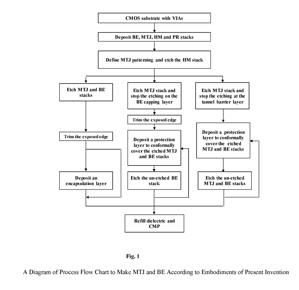
embodiment one
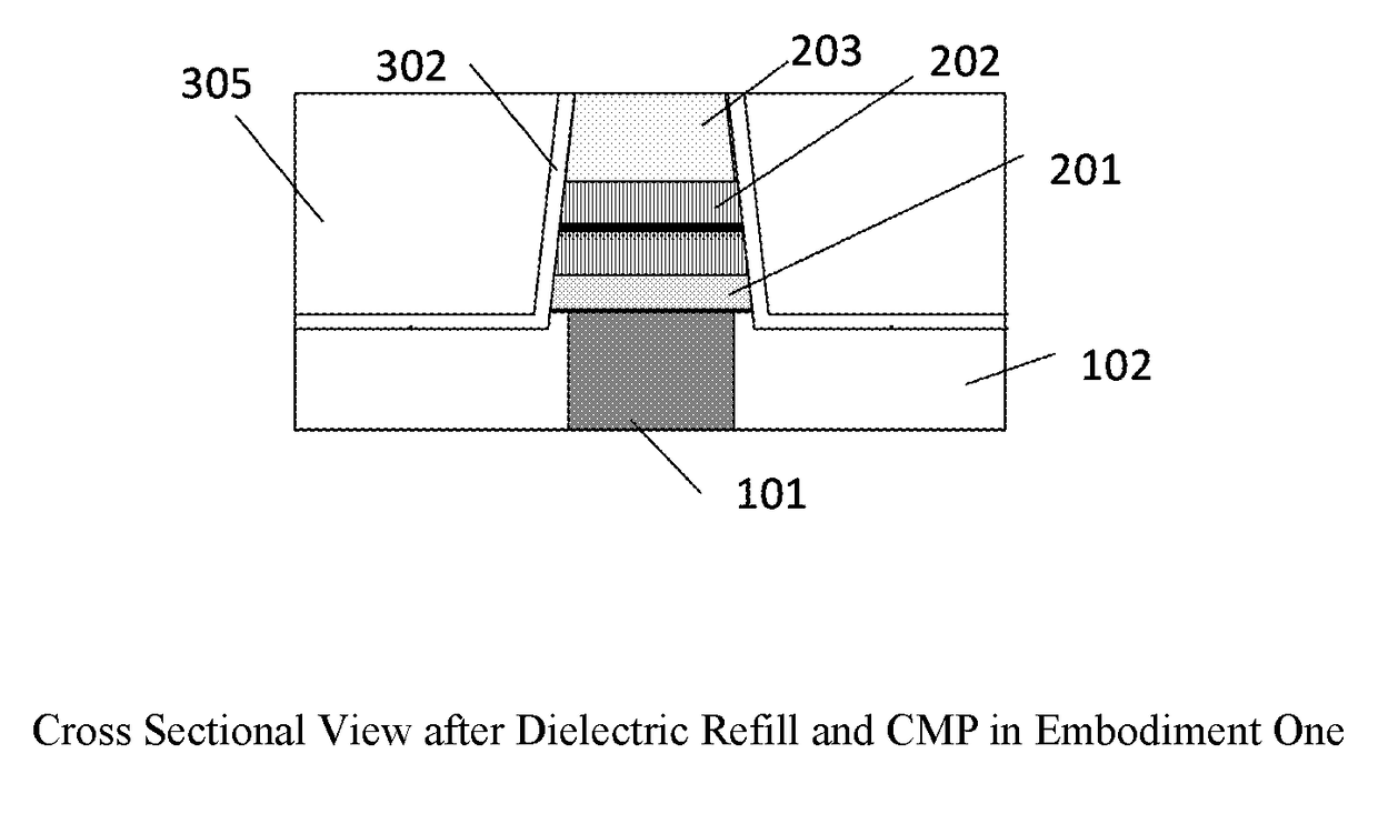
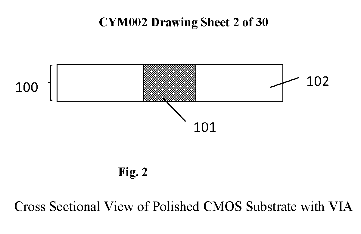
[0037]Following from the above HM stack (203) etch process, as shown in FIG. 5A, the MTJ (202) and BE (201) stacks are etched using one or more of RIE and / or IBE processes with Ta as hard mask (self-aligned etching process). A thin layer of IMD (101) under BE stack (201) should be etched away to prevent the electrical shorting between the bottom electrodes nearby.
[0038]The RIE etch process is taken place in an Inductively Coupled Plasma (ICP) or Capacitively Coupled Plasma (CCP) chamber with a precisely controllable vacuum range from 1 mTorr to 100 mTorr; The source power is adjusted from 200 watt to 3000 watt, the bias power is adjusted from 100 watt to 1500 watt; The main etchant of RIE could be selected from CH4 / H2, CO / NH3, CH3OH or C2H5OH with the gas flow rate from 5 sccm to 100 sccm, optionally, the RIE etchant could be also added by some other chemistries, such us: Ar, Kr and Xe etc., with the gas flow rate from 10 sccm to 200 sccm; The temperature range of Electrostatic Chuc...
embodiment two
[0044]Following from the above HM stack (203) etch process, as shown in FIGS. 6A and 6B, the MTJ stack (202) is etched and the etching is stopped on the capping layer of BE (201), then a low energy IBE trimming is used to remove the re-deposition and / or damage layer (301) on the exposed edge.
[0045]The etchant of MTJ stack (202) RIE could be selected from CO / NH3, CH3OH, CH3OH / Ar or C2H5OH, the endpoint trigger signal could be selected from OES or SIMS which could help to determine ending of etching using the changed signal at the interface of MTJ (202) and BE (201) capping layer. The trimming gas of IBE could be selected from Ar, Kr or Xe; The incident angle to the wafer stage could be selected from 0° to 90°, such us: 5° or 15°, etc.; The rotation speed of wafer stage is from 0 rpm to 60 rpm, such us: 15 rpm or 45 rpm. Optionally small flow of O3 or O2 could be also further used after the IBE trimming to oxidize any remaining metallic particles near the MTJ barrier.
[0046]Next, as sh...
embodiment three
[0055]Following from the above HM stack (203) etch process, as shown in FIG. 7A, the MTJ stack (202) is partially etched and the etching is stopped at the oxide tunnel barrier layer (2022) by using an endpoint detection.
[0056]The etchant of MTJ stack (202) RIE could be selected from CO / NH3, CH3OH, CH3OH / Ar or C2H5OH; The endpoint trigger signal could be selected from OES or SIMS which could help determine ending of etching using the changed signal at the tunnel barrier layer (2022).
[0057]Next, as shown in FIGS. 7B, 7C, 7D, 7E, 7F, 7G, 7H and 7I, the remaining un-etched portion of the MTJ stack (202) and BE stack (201) are etched using one or more of RIE and / or IBE processes with Ta & sidewall protection layer on top portion of MTJ as hard mask (self-aligned etching process). A thin layer of IMD (101) under BE stack (201) should be etched away to prevent the electrical shorting between the bottom electrodes nearby.
[0058]The self-aligned etching process of the remaining un-etched MTJ ...
PUM
 Abstract
Description
Claims
Application Information