Electro-mechanic-photonic delay line for analog signal processing

Active Publication Date: 2018-02-01
PSQUARED TECH LLC
View PDF0 Cites 23 Cited by
  • Summary
  • Abstract
  • Description
  • Claims
  • Application Information

AI Technical Summary

Benefits of technology

[0012]According to one aspect of the invention, there is provided a photonic modulator. The photonic modulator includes a transducer element that receives a RF input signal and converts the RF input signal into an elastic wave. One or more optical waveguides receive the elastic wave that has propagated a specified distance through an acoustic delay line. The one or more optical waveguides perform optomechanical transduction on the elastic wave in the presence of an optical wave, which produces one or more scattered optical waves. An optical circuit sums the one or more scattered waves to produce an optical signal output.
[0013]According to another aspect of the invention, there is provided a method of performing electro-acoustic optical modulation. The method includes receiving a RF input signal and converts the RF input signal into an elastic wave using a transducer element. Also, the method includes receiving the elastic wave that has propagated a specified distance through an acoustic delay line. The one or more optical wavegui

Problems solved by technology

However, there is a lack of compact tunable delay lines at microsecond level while being tunable, in terms of amplitude, phase and delay, and also being integratable in array forms on a semiconductor chip.
Integrated RF-photonics can pack such centimeter-long delay line on a millimeter-scale chip, but only allows fixed delay.
Surface-acoustic wave technology has similar limitations.
However, several major issues have plagued RF transmission line, which in turn triggered the birth of analog RF photonics in 1980s.
RF transmission lines produce 3.3-μs delay per kilometer of length: hundreds of meters of cable are required for μs-level delay (typical for self-cancellation application), which are typically bulky and too costly in practice.
RF transmission lines also exhibit higher losses at higher frequencies, due to the skin-effect and proximity effect, limiting the practical use of such RF delay lines to frequencies below 1 GHz.
In addition, the phase response of RF cables are vibration-sensitive, and most RF transmission lines are susceptible to electromagnetic interference.
Adding to these difficulties, adjustable delay is costly to realize due to the size and power required by RF switches.
Clearly, packing μs-level delays on a millimeter-sized chip still represents a major challenge: one needs to accommodate hundreds of meters of waveguides and more than 10 dB/μs on-ch

Method used


Image

  • Electro-mechanic-photonic delay line for analog signal processing
  • Electro-mechanic-photonic delay line for analog signal processing
  • Electro-mechanic-photonic delay line for analog signal processing

Examples


Embodiment Construction

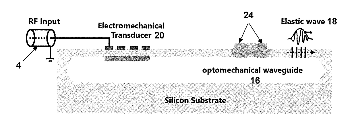
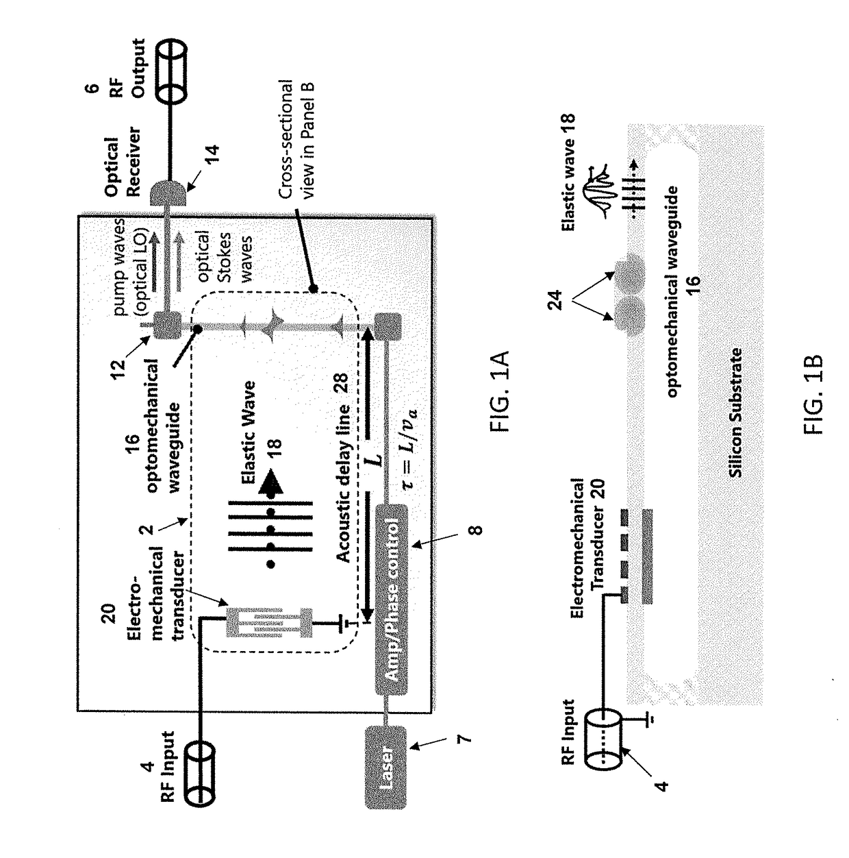
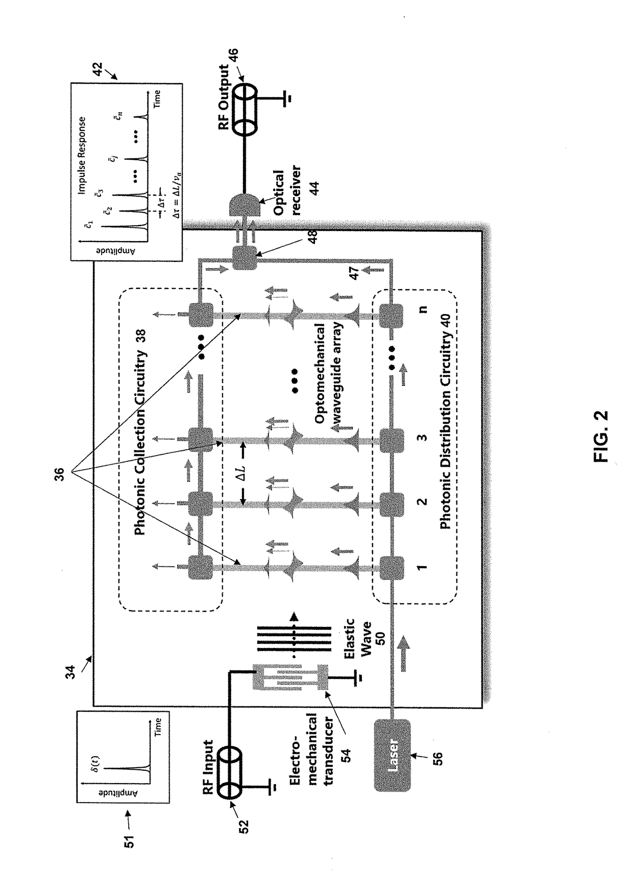
[0021]The invention involves a Reconfigurable Electro-Acousto-Photonic (REAP) modulator with built-in microsecond true time delay. Based on a new form of engineer-able on-chip electro-acousto-photonic coupling, this novel modulator enables RF signal processing with an unprecedented combination of ultra-wideband operation (UWB), rapid tunability, frequency agility, and ultra-compact footprint. Cascaded or parallelized arrays of such modulators can function as UWB finite-impulse-response filters, self-interference cancellation (SiC) filters, and correlators. This new chip-scale system performance levels are beyond the physical limits of similar structures in the prior art.

[0022]The Reconfigurable Electro-Acousto-Photonic (REAP) modulator is enabled by a unique hybridization between electro-mechanical, optomechanical, and microwave-photonic coupling. Distinct electromechanical, acoustic, optomechanical, and photonic building blocks that work together to produce the unprecedented combin...


PUM


Abstract

A photonic modulator is provided that includes a transducer element that receives a RF input signal and converts the RF input signal into an elastic wave. One or more optical waveguides receive the elastic wave that has propagated a specified distance through an acoustic delay line. The one or more optical waveguides perform optomechanical transduction on the elastic wave in the presence of an optical wave, which produces one or more scattered optical waves. An optical circuit sums the one or more scattered waves to produce an optical signal output.

Description

PRIORITY INFORMATION[0001]This application claims priority from provisional application Ser. No. 62 / 368,698 filed Jul. 29, 2016, which is incorporated herein by reference in its entirety.BACKGROUND OF THE INVENTION[0002]The invention relates to the field of electro-optic modulators, and in particular to a novel high-dynamic-range ultra-wideband (UWB) chip-scale modulator with built-in tunable microsecond true time delay.[0003]Current state-of-the-art chip-scale analog modulator technology generally provides negligible true time delay, and thus dedicated analog delay lines must be employed. However, there is a lack of compact tunable delay lines at microsecond level while being tunable, in terms of amplitude, phase and delay, and also being integratable in array forms on a semiconductor chip. For example, to cancel the echo effects from environmental scatterers, the analog cancellation filter in full-duplex transceivers demand larger numbers of taps in FIR configurations. And each ta...

Claims


Application Information

Patent Timeline
IPC IPC(8): H04B10/516H04B10/60H04B10/2575H04B10/50
CPCH04B10/516H04B10/2575H04B10/60H04B10/501G02F1/11
Inventor RAKICH, PETER THOMASWANG, ZHENG
Owner PSQUARED TECH LLC
Why Eureka
Try Eureka