Method of forming a solder bump structure

a technology of solder bumps and solder joints, which is applied in the direction of printed element electric connection formation, conductors, and single bars/rods/wires/strips, etc., can solve the problems of high process cost, difficult process management of electroless plating, and relatively high production cos

Active Publication Date: 2018-03-01
INT BUSINESS MASCH CORP
View PDF4 Cites 7 Cited by
  • Summary
  • Abstract
  • Description
  • Claims
  • Application Information

AI Technical Summary

Benefits of technology

[0007]The surface of the formed metal pillars (conductive layer) has cone-shaped surface. The cone-shaped surface covers the sidewalls of the openings of the resist layer, and extends upwardly to the entrance opening. Therefore, the contact area with solder formed thereon increases. Furthermore, it is possible to prevent the gas out from the side wall of the resist layer during solder melting (bonding) and the occurrence of incomplete solder fill.

Problems solved by technology

In that case, there is a problem of failure due to stress applied to the junction or failure due to electro migration (EM) caused by the increase of current density.
Therefore, the production cost is relatively high.
However, the electroless plating is difficult to process management.
Thus, the formation of the conventional solder bumps needs electroplating / electroless plating that the process cost is high and the process management is difficult.

Method used


Image

  • Method of forming a solder bump structure
  • Method of forming a solder bump structure
  • Method of forming a solder bump structure

Examples


embodiment 1

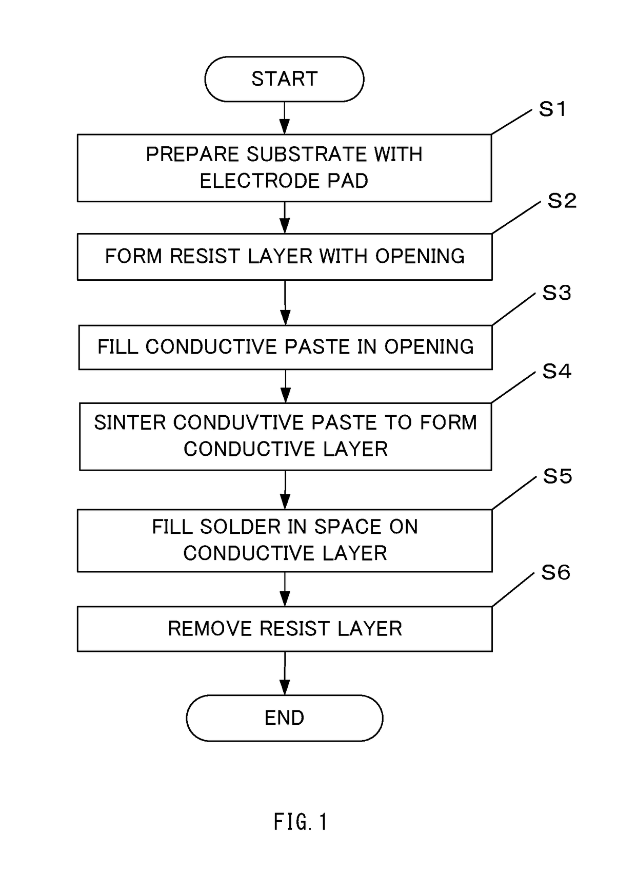
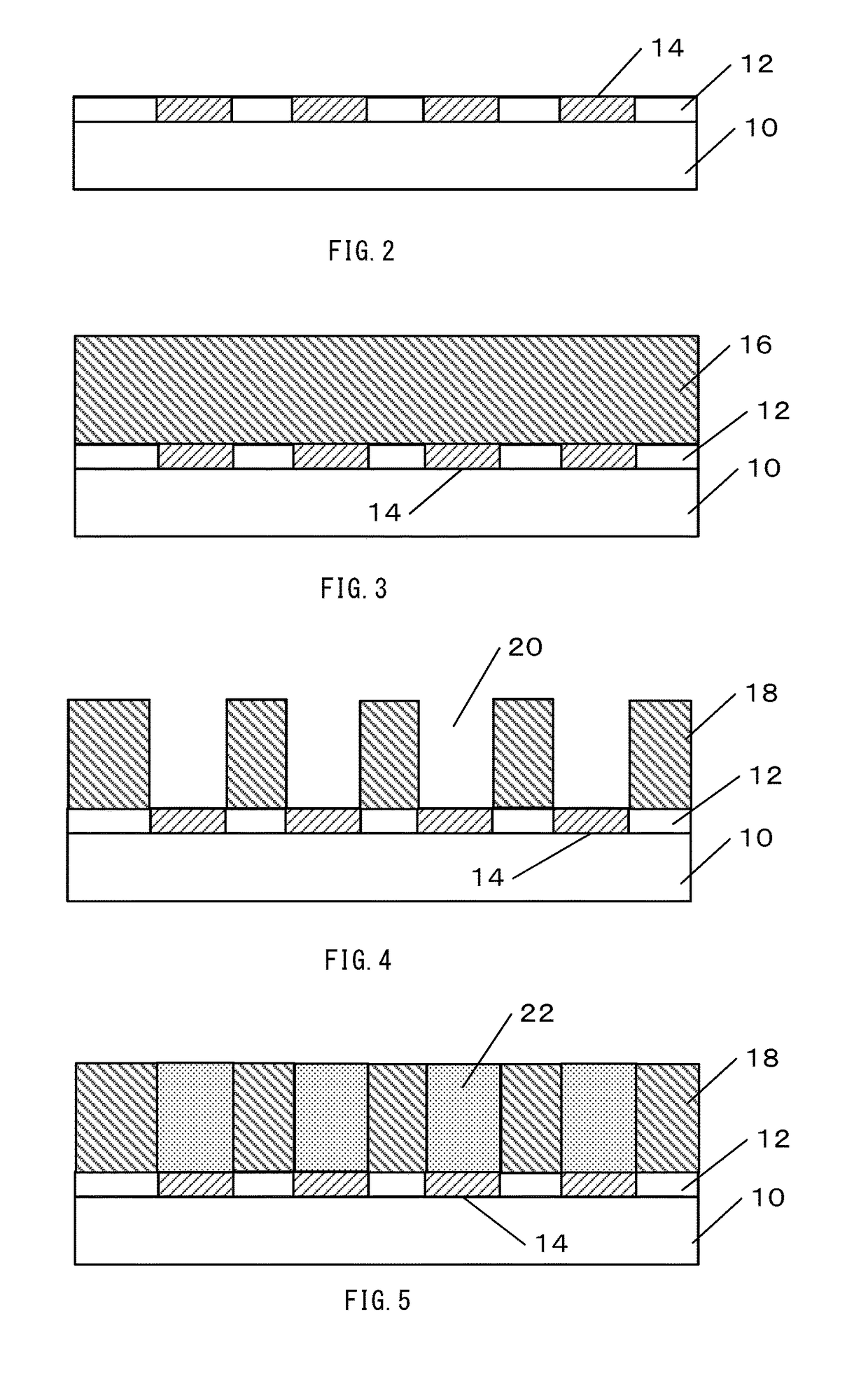
[0021]Referring FIG. 1 and FIG. 2, in step S1, a substrate 10 is prepared first. The substrate 10 has a surface on which electrode pads 14 have been formed between patterned insulating layers 12. The electrode pads 14 can include metal such as Aluminum (Al), for example. The insulating layers 12 can include silicon oxide (SiO2), for example. The substrate 10 can include semiconductor wafer such as a Si wafer, a semiconductor chip / die, or a circuit board. The material of the semiconductor wafer or chip is not limited to specific types. The substrate 10 can include a plurality of wiring layers (including circuits, devices such as a transistor) and insulating layers. The wiring layers can electrically connected to the electrode pads 14. The substrate 10 may include the lamination (stack) of a plurality of semiconductor substrates.

[0022]Referring FIG. 3, in step S2, a resist layer 16 is formed on the substrate 10 as shown in FIG. 3. A resist material is applied on the substrate 10 using...

embodiment 2

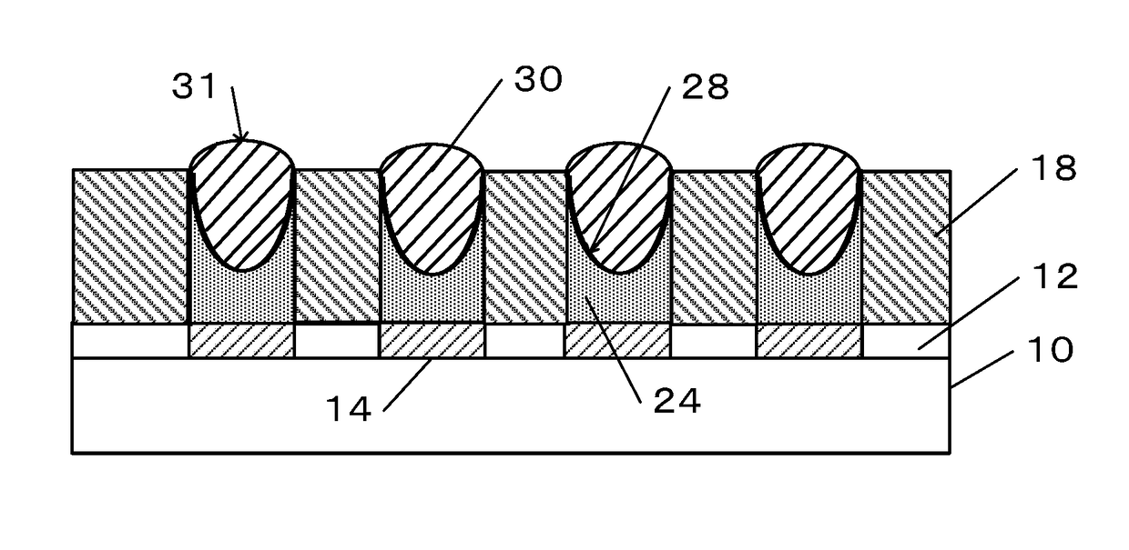
[0028]Referring FIG. 9 to FIG. 12, another embodiment of the method of the present invention is explained. Steps S10 to S40 in FIG. 9 are same as steps S1 to S4 in FIG. 1 as described above. Steps 50 to 70 are added as new steps in FIG. 9. FIG. 10 shows a cross-sectional diagram after step S40 which performs sintering of the conductive paste 22 in the opening 20 in FIG. 5. In FIG. 10, a thin conductive layer 34 is formed after the sintering process. The thin conductive layer 34 covers the side wall of the resist layer 18 and the surface of the electrode pad 14 in the opening 20 as shown in FIG. 10. The thickness TC1 of the central portion 35 of the conductive layer 34 is thinner than the predetermined thickness in the range of 1 to 50 micrometers, for example. Therefore, it is necessary to form additional conductive layers on the conductive layer 34 in order to ensure a predetermined thickness.

[0029]In step S50, additional conductive paste 36 is filled in the opening 26 of the resis...

embodiment 3

[0031]Referring FIG. 1, FIG. 5, and FIG. 7, another embodiment of the method of the present invention is explained. In this embodiment, the filling of the conductive paste 22 in step S3 of FIG. 1 and FIG. 5 is performed using IMS process which is used in step S5 of filling of solder 30 instead of screen printing. In step S3, the conductive paste 22 is injected in place of solder under predetermined pressure by IMS process. By using the IMS in Step S3, it is possible to perform steps S3 to Step S5 under one IMS process. That is, even sintering of step S4 can be performed in the IMS process. As a result, it is possible to achieve a further shortening of the production time and simplification of the manufacturing process to form the solder bump structure.

[0032]The embodiment of the present invention has been described with reference to the accompanying drawings. However, the present invention is not limited to the embodiment. The present invention can be carried out in forms to which v...


PUM

PropertyMeasurementUnit
thicknessaaaaaaaaaa
volume shrinkageaaaaaaaaaa
thicknessaaaaaaaaaa

Abstract

A method of the present invention includes preparing a substrate having a surface on which a electrode pad is formed, forming a resist layer on the substrate, the resist layer having an opening on the electrode pad, filling conductive paste in the opening of the resist layer; sintering the conductive paste in the opening to form a conductive layer which covers a side wall of the resist layer and a surface of the electrode pad in the opening, a space on the conductive layer leading to the upper end of the opening being formed, filling solder in the space on the conductive layer and removing the resist layer.

Description

BACKGROUND OF THE INVENTIONTechnical Field[0001]The present invention relates to a method of forming a solder bump structure, and more specifically, to a method of forming a solder bump structure using metal paste and molten solder.Description of the Related Art[0002]While performance and function of electronics devices improve highly, the flip chip packaging is broadly applied from the consumer product represented by a smart phone, tablet PC, etc. to the supercomputer. Furthermore, it is predicted that the demand of the flip chip packaging increases sharply by the appearance of the 2.5 or 3-dimensional (2.5D or 3D) stacked device of the semiconductor chip.[0003]In the 2.5D or 3D package, connecting terminals pitch and bump size is dramatically fine. In that case, there is a problem of failure due to stress applied to the junction or failure due to electro migration (EM) caused by the increase of current density. To solve this problem, the solder bumps using Cu pillars corresponding...

Claims


Application Information

Patent Timeline
Patent Type & Authority Applications(United States)
IPC IPC(8): H01L23/00H01B5/02H01B1/02H05K1/11H05K3/40
CPCH01L2224/13005H01L2924/01079H01L2924/01047H01L2924/01029H01L2924/01028H05K3/4007H01B5/02H01B1/026H05K1/111H01L24/13H01L24/11H01L24/05H01L2224/03831H01L2224/0401H01L2224/05567H01L2224/05624H01L2224/11312H01L2224/1132H01L2224/11505H01L2224/11622H01L2224/13018H01L2224/13076H01L2224/13082H01L2224/13109H01L2224/13111H01L2224/13113H01L2224/13339H01L2224/13344H01L2224/13347H01L2224/13355H01L2224/94H05K2201/10734H01L2224/11H01L2924/00014H01L2924/0105H01L2924/01083H01L2924/01049H01L2924/0103H01L2924/01027H01L2924/01032H01L2924/01026H01L2924/01022H05K3/3478
Inventor AOKI, TOYOHIROHISADA, TAKASHINAKAMURA, EIJI I.
Owner INT BUSINESS MASCH CORP
Why Eureka
Try Eureka