Method for manufacturing thin film transistor

a thin film transistor and manufacturing method technology, applied in the field of displays, can solve the problems of poor production and long production cycle, and achieve the effects of reducing the electron mobility, long production cycle, and large negative

Active Publication Date: 2018-03-22
WUHAN CHINA STAR OPTOELECTRONICS TECH CO LTD
View PDF0 Cites 0 Cited by
  • Summary
  • Abstract
  • Description
  • Claims
  • Application Information

AI Technical Summary

Benefits of technology

[0009]An object of the present invention is to provide a method for manufacturing a thin film transistor, which solves the problem of the conventional method for manufacturing a thin film transistor, which has a complicated process, a long production cycle and a large negative effect for the uniformity of ion implantation, that may lower the electron mobility of the heavily doped drain region and the lightly doped drain region.

Problems solved by technology

As described above in the method for manufacturing a thin film transistor, the lightly doped drain region is formed by forming two photoresist patterns, which is a complicated process, and has long production cycle, and is not good for production.

Method used


Image

  • Method for manufacturing thin film transistor
  • Method for manufacturing thin film transistor
  • Method for manufacturing thin film transistor

Examples


Embodiment Construction

[0050]The structure and the technical means adopted by the present invention to achieve the above and other objects can be best understood by referring to the following detailed description of the preferred embodiments and the accompanying drawings. Furthermore, directional terms described by the present invention, such as upper, lower, front, back, left, right, inner, outer, side, longitudinal / vertical, transverse / horizontal, etc., are only directions by referring to the accompanying drawings, and thus the used directional terms are used to describe and understand the present invention, but the present invention is not limited thereto.

[0051]Below with reference to the accompanying drawings and described in detail with an embodiment of the present invention.

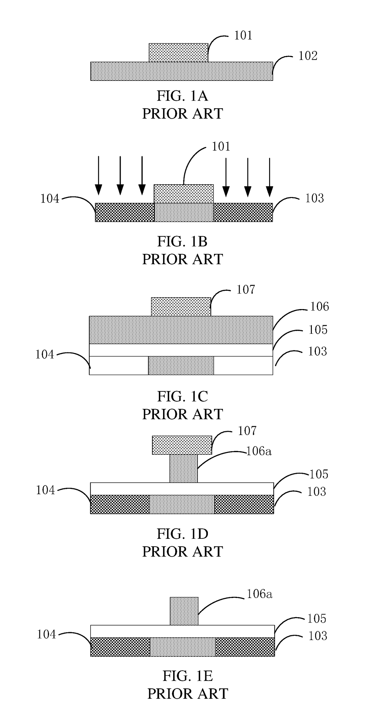
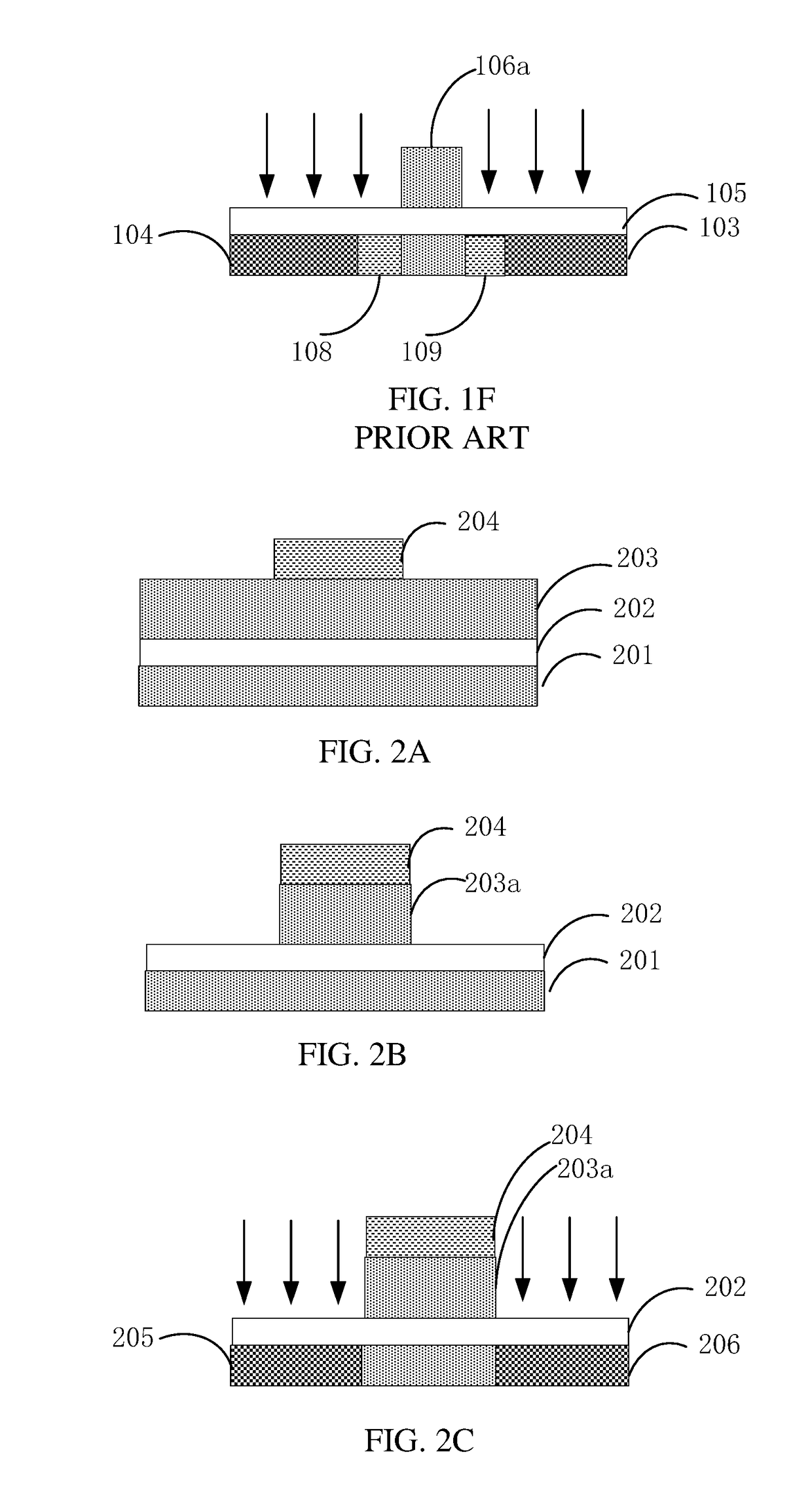
[0052]It is improved that a complex process of a thin film transistor resulting a long production cycle.

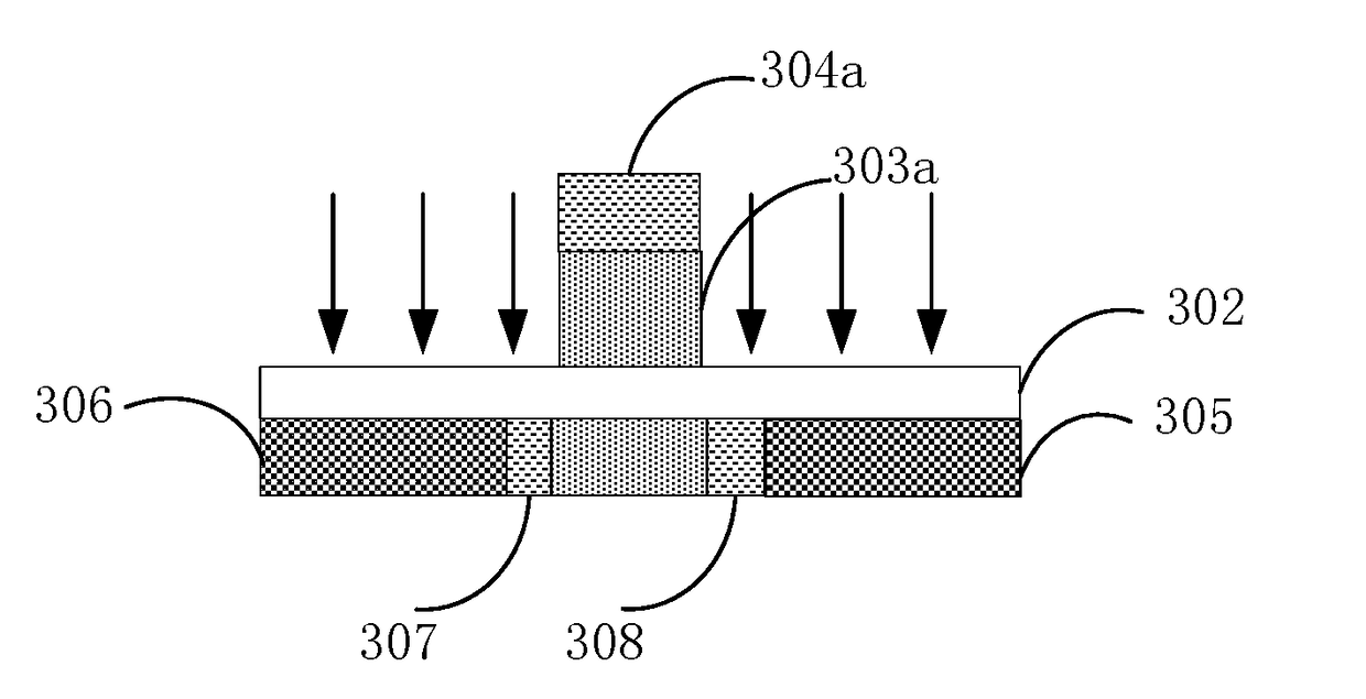
[0053]Refer to FIGS. 2A to 2F, which are a flow chart of a method for manufacturing the thin film transistor of the present i...


PUM


Abstract

A method for manufacturing a thin film transistor is provided. The method comprises depositing sequentially a gate insulating layer and a gate metal layer on a semiconductor substrate; etching the gate metal layer uncovered by the first photoresist pattern; implementing a first ion implantation on the semiconductor substrate; etching a side wall of the first photoresist pattern; implementing a second ion implantation on the semiconductor substrate to form a source and a drain. The source and the drain include a heavily doped drain region and a lightly doped drain region.

Description

FIELD OF THE INVENTION[0001]The present invention relates to a technical field of displays, and in particular to a method for manufacturing a thin film transistor.BACKGROUND OF THE INVENTION[0002]A method for manufacturing a low-temperature polycrystalline silicon thin film is a new generation method of a thin film transistor liquid crystal display, which is an a-Si film changed to a polysilicon thin film layer through aLaser annealing process. The polysilicon thin film layer is used to form thin film transistors of data lines and scan lines in the liquid crystal display panel. The moving velocity of electrons of polysilicon thin film transistors is one hundred times faster than amorphous silicon elements. Therefore, rapid response of the liquid crystal display panel, highlight display, and high resolution can be implemented.[0003]Refer to FIGS. 1A to 1F, which are schematic views of a traditional method for manufacturing the thin film transistor.[0004]Refer to FIG. 1A, a first phot...

Claims


Application Information

Patent Timeline
Patent Type & Authority Applications(United States)
IPC IPC(8): H01L29/66H01L21/265H01L21/3213H01L21/311
CPCH01L29/66757H01L21/26513H01L21/32135H01L21/32139H01L21/31138H01L29/66765H01L29/78678H01L29/78621
Inventor YE, JIANGBO
Owner WUHAN CHINA STAR OPTOELECTRONICS TECH CO LTD
Why Eureka
Try Eureka