Storage device, driving method thereof, semiconductor device, electronic component, and electronic device
a driving method and storage device technology, applied in the direction of static storage, digital storage, instruments, etc., can solve the problems of increasing the difficulty of keeping required capacitance, and achieve the effect of improving noise margin and reducing incorrect data reading
- Summary
- Abstract
- Description
- Claims
- Application Information
AI Technical Summary
Benefits of technology
Problems solved by technology
Method used
Image

Examples
embodiment 1
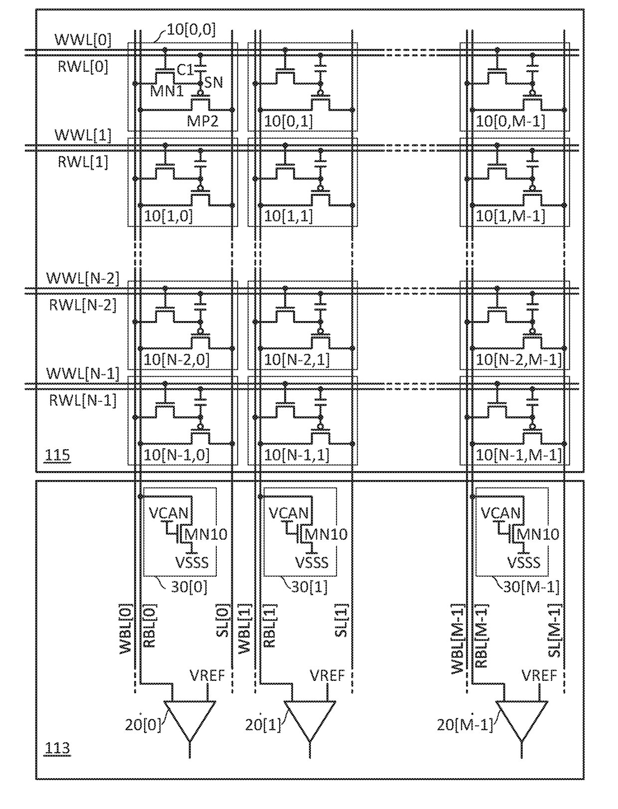
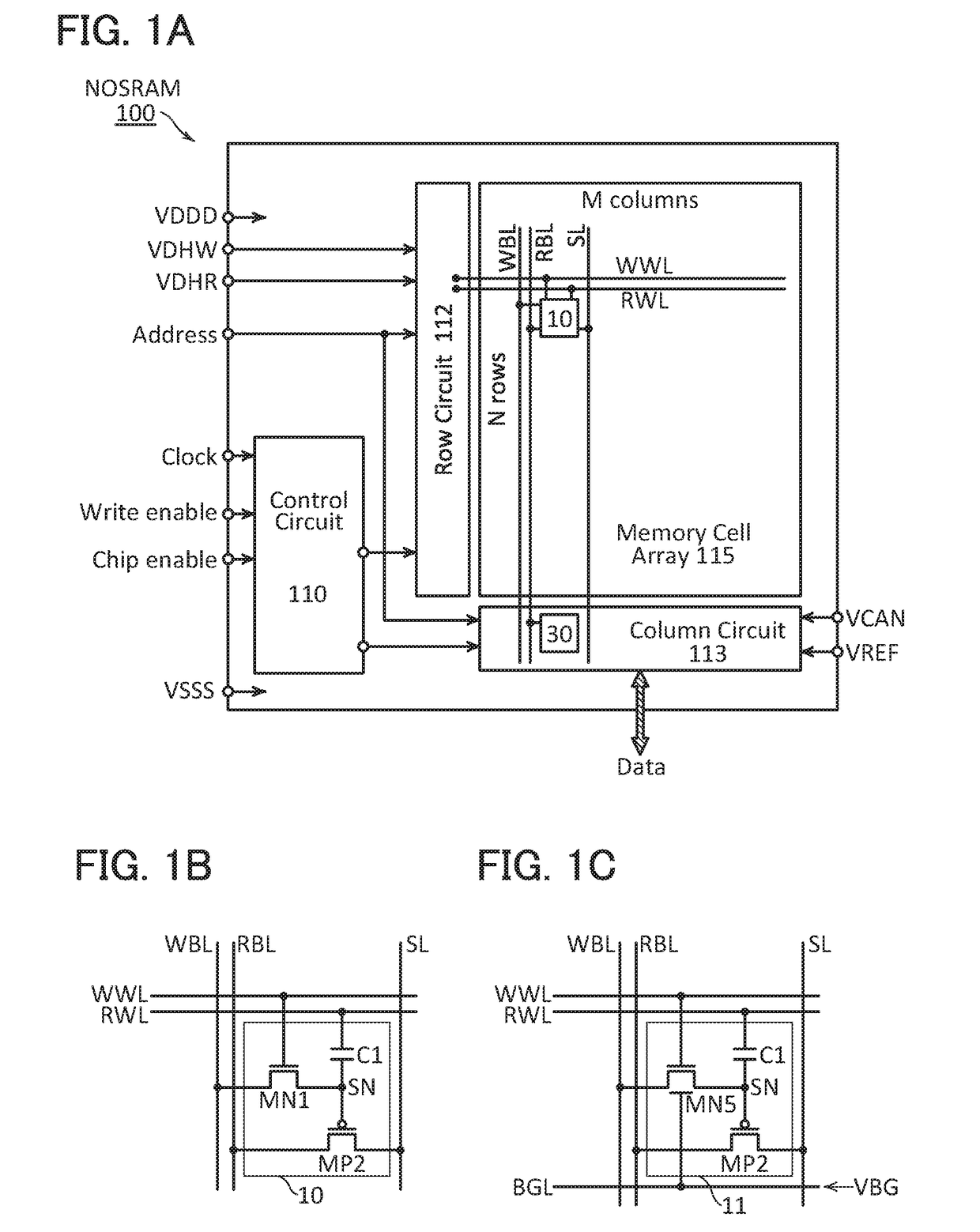
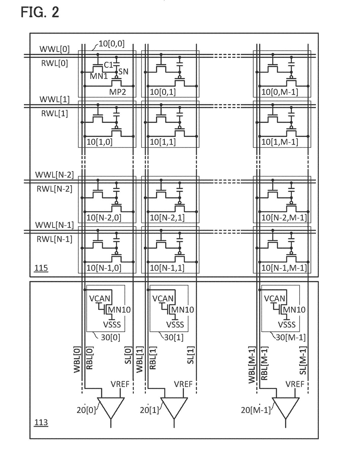
[0059]In this embodiment, a storage device including a gain-cell memory cell is described. A NOSRAM is described here as an example of such a storage device.
100>
[0060]FIG. 1A is a block diagram illustrating a structure example of a NOSRAM. A NOSRAM 100 includes a control circuit 110, a row circuit 112, a column circuit 113, and a memory cell array 115. Potentials VDDD, VSSS, VDHW, VDHR, VCAN, and VREF, a clock signal, an address signal, a chip enable signal, and a write enable signal are input from the outside to the NOSRAM 100.
[0061]The control circuit 110 has a function of controlling the entire operation of the NOSRAM 100. For example, the control circuit 110 performs logical operation of the chip enable signal and the write enable signal and determines whether access from the outside is write access or read access.
[0062]The row circuit 112 has a function of selecting a word line in a row specified by the address signal. The column circuit 113 has a function of writing and readin...
embodiment 2
[0129]FIG. 8 is a block diagram illustrating a structure example of a NOSRAM. A NOSRAM 200 includes a control circuit 201, a predecoder 202, a row circuit 203, a column circuit 204, and a memory cell array 205. The memory cell array 205 includes cells 40, the word lines WWL and RWL, the bit lines WBL and RBL, and the source line SL.
[0130]The potentials VDDD, VSSS, VDHW, VDHR, VCAN, VREF, and VBG are input to the NOSRAM 200.
[0131]The signals CLK, CE, GW, and BW, and signals BURST and ADDR are input to the NOSRAM 200. The signal CLK is a clock signal. The signal CE is a chip enable signal. The signal GW is a global write enable signal. The signal BW is a byte write enable signal. The signal BURST is a burst signal controlling burst operation. The signal ADDR is an address signal. Data WDA is write data input from the outside. Data RDA is read data output from the NOSRAM 200.
[0132]The circuits, signals, and potentials in the NOSRAM 200 can be selected as appropriate. Another circuit or...
embodiment 3
[0176]FIG. 13A a is a block diagram illustrating a structure example of a NOSRAM. A NOSRAM 300 includes a memory cell array, a control circuit 301, a predecoder 302, four row circuits 303[00] to 303[11], and two column circuits 304[0] and 304[1]. The memory cell array in the example of FIG. 13A is divided into four. Here, the four memory cell arrays are referred to as blocks 305[00] to 305[11].
[0177]A row circuit 303M is a row circuit of a block 305[XX] (X is 0 or 1). One column circuit 304 is used in common between two blocks 305. The column circuit 304[0] is used in common between the blocks 305[00] and 305[10]. The column circuit 304[1] is used in common between the blocks 305[01] and 305[11].
[0178]The NOSRAM 300 is supplied with the signals CLK, CE, GW, BW[3:0], BURST, and ADDR, and the data WDA[31:0] and outputs the data RDA[31:0]. The potentials VDDD, VSSS, VDHW, VDHR, VCAN, and VBG and potential VDUM are input to the NOSRAM 300.
[0179]The circuits, signals, and potentials in t...
PUM
 Abstract
Description
Claims
Application Information