Compound for organic electric element, organic electric element comprising the same and electronic device thereof

a technology of organic electric elements and organic electric elements, which is applied in the direction of organic chemistry, solid-state devices, semiconductor devices, etc., can solve the problems of increasing power consumption, affecting efficiency and life span, and requiring more and more power consumption, so as to facilitate the charge balance and reduce the driving voltage of organic electric elements.

Pending Publication Date: 2018-05-03
DUK SAN NEOLUX
View PDF6 Cites 14 Cited by
  • Summary
  • Abstract
  • Description
  • Claims
  • Application Information

AI Technical Summary

Benefits of technology

[0015]According to the embodiments of the present invention, by using a specific compound as a material of the organic electric device, wherein the specific compound have the limited type of an amine group bonded to the linking group, and the limited bonding position and number of amine grou...

Problems solved by technology

Currently, the power consumption is required more and more as size of display becomes larger and larger in the portable display market.
Therefore, the power consumption is a very important factor in the portable display with a limited power source of the battery, and efficiency and life span issue also must be solved.
However, efficiency cannot be maximized only by simply improving the organic material layer.
However, when a material having a high hole mobility is used to lower a driving voltage, a positive polaron is accumulated at the interface ...

Method used


Image

  • Compound for organic electric element, organic electric element comprising the same and electronic device thereof
  • Compound for organic electric element, organic electric element comprising the same and electronic device thereof
  • Compound for organic electric element, organic electric element comprising the same and electronic device thereof

Examples


synthesis example

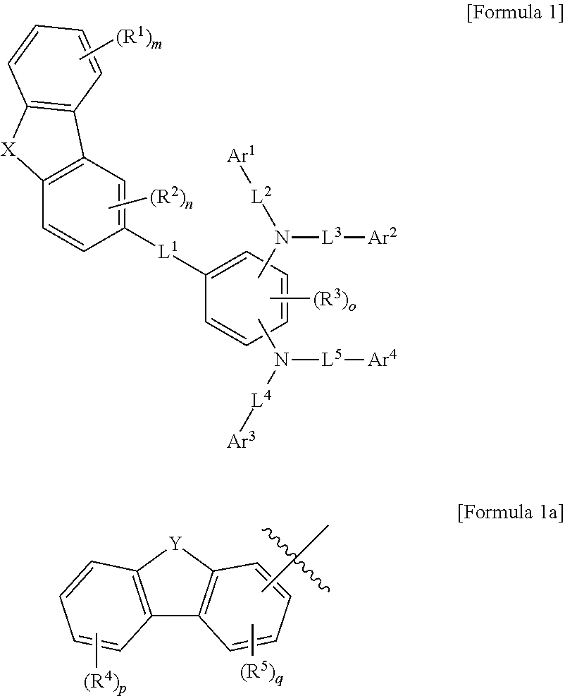
[0086]The compound(final products) represented by Formula 1 according to the present invention are synthesized by reacting Sub 1 and Sub 2 as shown in Reaction Scheme 1, but are not limited thereto.

[0087]In the above Reaction Scheme 1, symbols of X, R1 to R3, Ar1 to Ar4, L1 to L5, m, n, o or the like are each identical as defined in formula 1.

[0088]I. Synthesis of Sub 1

[0089]Sub 1 of the Reaction Scheme 1 can be synthesized according to, but not limited to, the following Reaction Schemes 2 to 5.

[0090]Synthesis Examples of compounds comprised in Sub 1 are as follows.

1. Synthesis Examples of Sub 1-1

[0091]

[0092](1) Synthesis of Sub 1-I-1

[0093]The starting material 5-bromo-2-(methylsulfinyl)-1,1′-biphenyl (63.18 g, 214.03 mmol) was placed into a round bottom flask together with triflic acid (284.1 ml, 3210.47 mmol) and stirred at room temperature for 24 hours. Then, a pyridine aqueous solution (3750 ml, pyridine: H2O=1:5) was slowly added dropwise, refluxed and stirred for 30 minutes. W...

example i-1

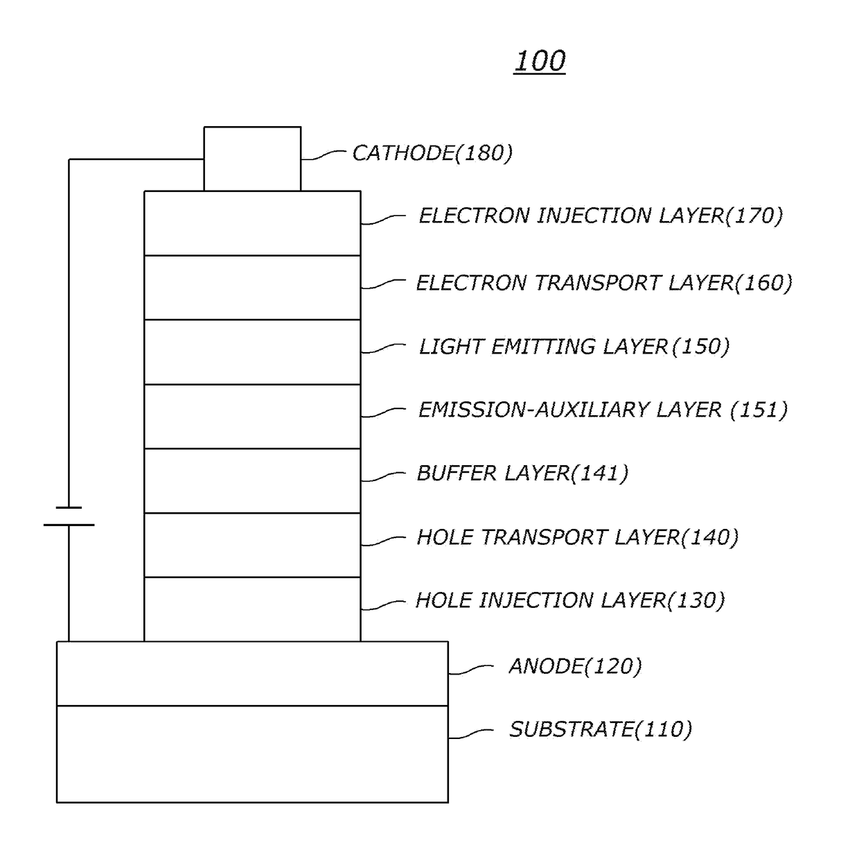
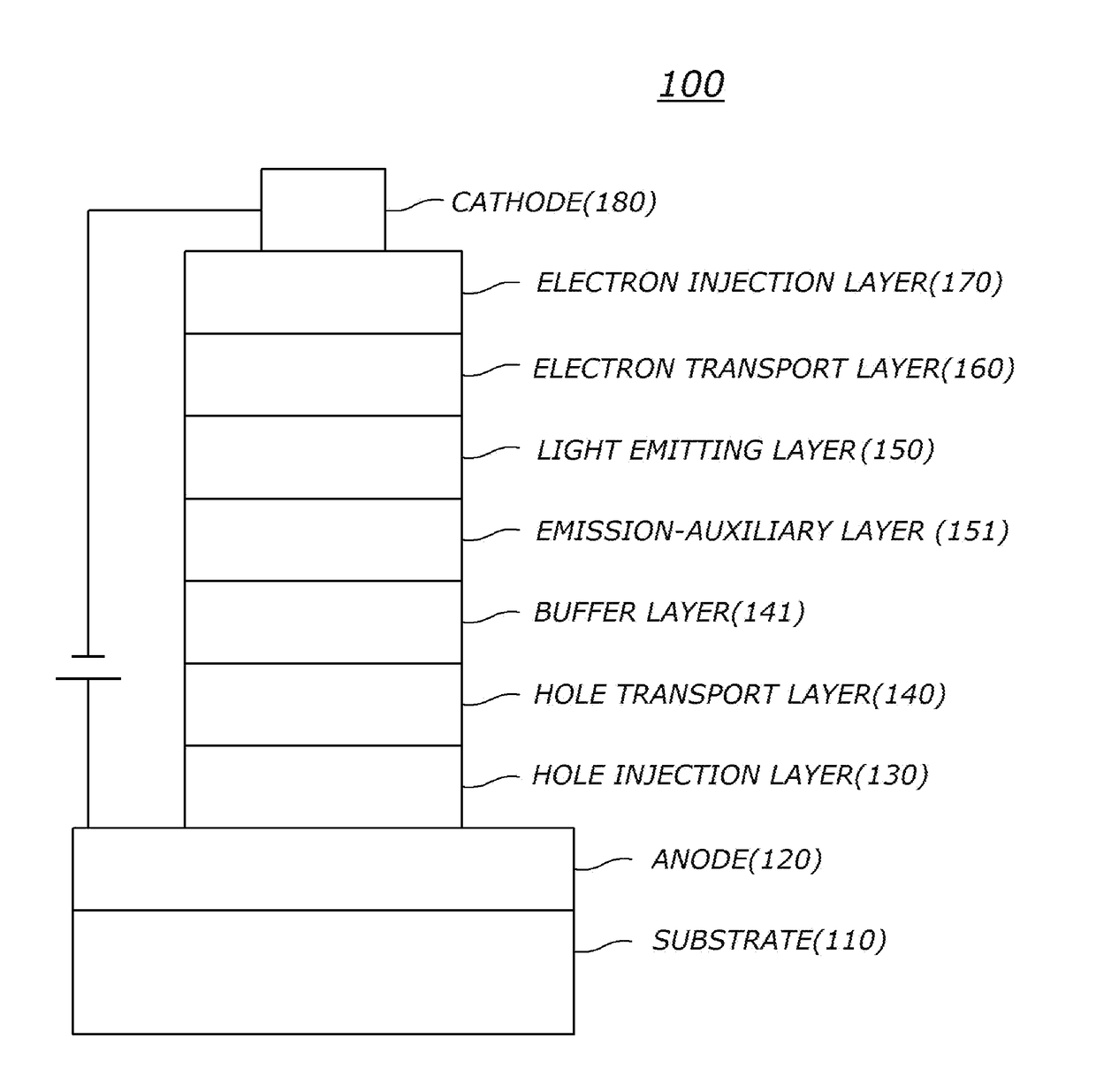
[Example I-1] Green OLED (A Hole Transport Layer)

[0251]Organic light emitting diodes (OLEDs) were fabricated according to a conventional method by using a compound of the present invention as a hole transport layer material.

[0252]First, an ITO layer (anode) was formed on a glass substrate, and then 4,4′,4″-tris[2-naphthyl(phenyl)amino]triphenylamine (hereinafter, “2-TNATA”) was vacuum-deposited on the ITO layer to form a hole injection layer with a thickness of 60 nm.

[0253]Subsequently, compound P-1 of the present invention was vacuum-deposited with a thickness of 60 nm on the hole injection layer to form a hole transport layer.

[0254]Subsequently, a light emitting layer with a thickness of 30 nm was formed on the hole transport layer by using 4,4′-N,N′-dicarbazole-biphenyl (hereinafter, “CBP”) as a host material and tris(2-phenylpyridine)-iridium (hereinafter, “Ir(ppy)3)”) as a dopant material in a weight ratio of 90:10.

[0255]Next, ((1,1′-bisphenyl)-4-olato)bis(2-methyl-8-quinolinol...

example i-2

[Example I-2] to [Example I-70] Green OLED (A Hole Transport Layer)

[0257]The OLEDs were fabricated in the same manner as described in Example I-1 except that the compounds P-2 to P-144 of the present invention described in Table 4 instead of the compound P-1 of the present invention were used as the hole transport layer material.

[Comparative Example I-1] to [Comparative Example I-7]

[0258]The OLEDs were fabricated in the same manner as described in Example I except that the following Comparative Compounds 1 to 7 described in Table 4 instead of the compound P-1 of the present invention were each used as the hole transport layer material.

[0259]Electroluminescence (EL) characteristics were measured with a PR-650(Photoresearch) by applying a forward bias DC voltage to the OLEDs prepared in Examples I-1 to I-70 of the present invention and Comparative Examples I-1 to I-7. And, the T95 life time was measured using a life time measuring apparatus manufactured by Macscience Inc. at reference...


PUM


Abstract

Provided are a compound represented by Formula 1, and an organic electric element comprising a first electrode, a second electrode, and an organic material layer formed between the first electrode and the second electrode, wherein the organic material layer comprised the compound represented by Formula 1, and the driving voltage of an organic electronic device can be lowered, and the luminous efficiency, color purity and life time of an organic electronic device can be improved by comprising the compound represented by Formula 1 in the organic material layer.

Description

CROSS-REFERENCE TO RELATED APPLICATION[0001]This patent application claims priority from and the benefit under 35 U.S.C. 119(a) of Korean Patent Application No. 10-2015-0051847, filed on Apr. 13, 2015, which is hereby incorporated by reference for all purposes as if fully set forth herein. Further, this application claims the benefit of priority in countries other than U.S.A, which is hereby incorporated by reference herein.BACKGROUNDTechnical Field[0002]The present invention relates to compounds for organic electric elements, organic electric elements comprising the same, and electronic devices thereof.Background Art[0003]In general, an organic light emitting phenomenon refers to a phenomenon in which electric energy is converted into light energy of an organic material. An organic electric element utilizing the organic light emitting phenomenon usually has a structure including an anode, a cathode, and an organic material layer interposed therebetween. In many cases, the organic m...

Claims


Application Information

Patent Timeline
IPC IPC(8): H01L51/00C07D409/10C07D333/76C07D333/50C07D407/12C07D407/14C07D409/14C07D307/77
CPCH01L51/0061C07D409/10C07D333/76C07D333/50H01L51/5206C07D407/14C07D409/14C07D307/77H01L51/006C07D407/12C07D307/91C07D307/93C07D333/78C07D409/12Y02E10/549H10K50/15H10K85/633H10K85/636H10K50/11H10K50/16H10K50/17H10K50/81H10K50/82H10K50/166H10K50/171H10K85/615H10K85/622H10K85/624H10K85/626H10K85/654H10K85/6572H10K85/6574H10K85/6576
Inventor SO, KIHOCHOI, YEONHEEKIM, DAESUNGLEE, YUNSUKPARK, JONGGWANGLEE, GA-EUNHWANG, SUNPIL
Owner DUK SAN NEOLUX
Why Eureka
Try Eureka