Chemically amplified resist composition and patterning process
- Summary
- Abstract
- Description
- Claims
- Application Information
AI Technical Summary
Benefits of technology
Problems solved by technology
Method used
Image
Examples
example
[0133]Examples of the invention are given below by way of illustration and not by way of limitation. The abbreviation “pbw” is parts by weight.
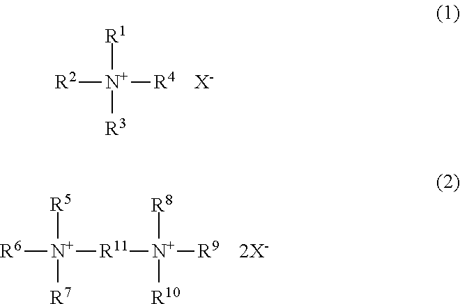
[0134]Quenchers 1 to 12 in the form of quaternary ammonium iodide, quaternary ammonium dibromoiodide, quaternary ammonium bromodiiodide or quaternary ammonium triiodide having the following structure were used in resist compositions. Of Quenchers 1 to 12, some were purchased from Tokyo Chemical Industry Co., Ltd. or Sigma-Aldrich and the remaining were prepared by neutralization reaction of an ammonium hydroxide with hydriodic acid.
synthesis example
[0135]Synthesis of Base Polymers (Polymers 1 to 3)
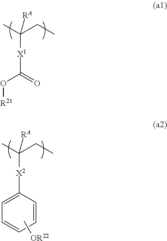
[0136]Base polymers were prepared by combining suitable monomers, effecting copolymerization reaction thereof in tetrahydrofuran (THF) solvent, pouring the reaction solution into methanol for crystallization, repeatedly washing with hexane, isolation, and drying. The resulting polymers, designated Polymers 1 to 3, were analyzed for composition by 1H-NMR spectroscopy, and for Mw and Mw / Mn by GPC versus polystyrene standards using THF solvent.
examples 1-1 to 1-16
and Comparative Examples 1-1 to 1-7
[0141]Each of the resist compositions (Tables 1 and 2) was spin coated onto a silicon substrate (which had been vapor primed with hexamethyldisilazane) and prebaked on a hotplate at 110° C. for 60 seconds to form a resist film of 80 nm thick. Using a system HL-800D (Hitachi Ltd.) at an accelerating voltage of 50 kV, the resist film was exposed imagewise to EB in a vacuum chamber. Immediately after the exposure, the resist film was baked (PEB) on a hotplate at the temperature shown in Tables 1 and 2 for 60 seconds and developed in a 2.38 wt % TMAH aqueous solution for 30 seconds to form a pattern.
[0142]The resist pattern was evaluated as follows. In the case of positive resist film, the resolution is a minimum trench size at the exposure dose that provides a resolution as designed of a 120-nm trench pattern. In the case of negative resist film, the resolution is a minimum isolated line size at the exposure dose that provides a resolution as designed...
PUM
| Property | Measurement | Unit |
|---|---|---|
| Nanoscale particle size | aaaaa | aaaaa |
| Nanoscale particle size | aaaaa | aaaaa |
| Wavelength | aaaaa | aaaaa |
Abstract
Description
Claims
Application Information


