Metal oxide thin-film transistor and manufacturing method for the same
- Summary
- Abstract
- Description
- Claims
- Application Information
AI Technical Summary
Benefits of technology
Problems solved by technology
Method used
Image
Examples
first embodiment
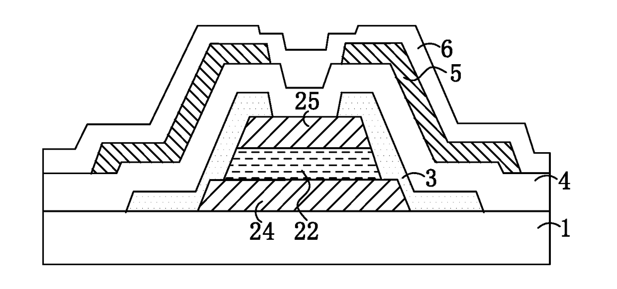
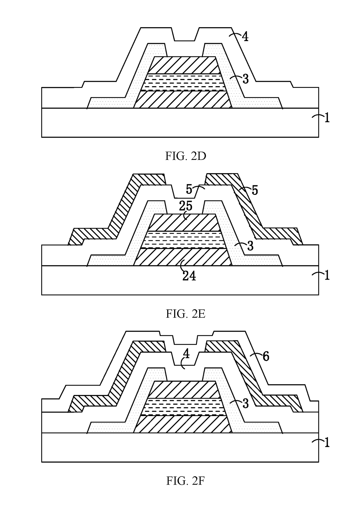
[0066]The present embodiment provides a manufacturing method for a metal oxide thin-film transistor, comprising following steps:
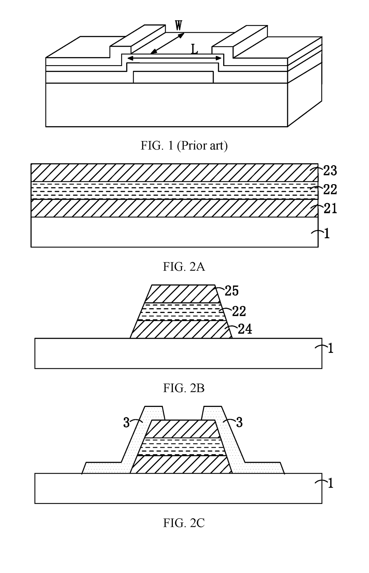
[0067]As shown in FIG. 2A, preparing a substrate 1, and through a sputtering method to sequentially deposit a first metal layer 21, a barrier layer 22 and a second metal layer 23. Wherein, each of the first metal layer and the second metal layer adopts metal molybdenum (Mo), and the barrier layer adopts a SiOx material. In the present embodiment, the barrier layer can be an insulation layer, or a semiconductor layer having a higher resistance, that is, a semiconductor layer with high resistance. When the barrier layer is an insulation layer, a SiNx material can also be adopted. When the barrier layer is a semiconductor layer with high resistance, a ZnO based, a SnO2 based or an In2O3 based transparent oxide semiconductor material can be adopted. Each of the first metal layer and the second metal layer can also adopt other metal materials such as metal mater...
second embodiment
[0077]The difference between the present embodiment and the first embodiment is that, as shown in FIG. 4A, after performing a photolithography process to the first metal layer, the barrier layer and the second metal layer, from a cross-sectional structure of the metal oxide thin-film transistor, the drain electrode 25 after photolithography process are respectively located at left and right sides of an upper surface of the barrier layer 22 such that a middle portion of the upper surface of the barrier layer 22 is exposed. At the same time, as shown in FIG. 4B, from a top view of a plane structure of the metal oxide thin-film transistor, the drain electrode located at a left side and the drain electrode located at a right side are connected. It can be understood that, in order to clearly show the connection property of the drain electrode in the plane structure of the metal oxide thin-film transistor, in FIG. 4B, only partial main structures of the metal oxide thin-film transistor ar...
third embodiment
[0079]The difference between the present embodiment and the manufacturing method in the first embodiment is that, when performing a photolithography process to the first metal layer, the barrier layer and the second metal layer, a grayscale mask is adopted for exposing and developing. Finally, as shown in FIG. 5, from a cross-sectional structure of the metal oxide thin-film transistor, a lower surface of the barrier layer 22 only covers a portion of the source electrode, after the photolithography process, a length of an upper surface of the source electrode 24 is greater than a length of a lower surface of the barrier layer 22. That is, a left side and a right side of the source electrode 24 are respectively protruded from the barrier layer 22 and the drain electrode 25, and are exposed outside a covering range of the barrier layer 22 and the drain electrode 25.
[0080]The metal oxide thin-film transistor obtained by the manufacturing method of the present embodiment, from the cross-...
PUM
 Abstract
Description
Claims
Application Information
 - R&D Engineer
- R&D Manager
- IP Professional
- Industry Leading Data Capabilities
- Powerful AI technology
- Patent DNA Extraction
Browse by: Latest US Patents, China's latest patents, Technical Efficacy Thesaurus, Application Domain, Technology Topic, Popular Technical Reports.
© 2024 PatSnap. All rights reserved.Legal|Privacy policy|Modern Slavery Act Transparency Statement|Sitemap|About US| Contact US: help@patsnap.com


