Method to improve adhesion of photoresist on silicon substrate for extreme ultraviolet and electron beam lithography

a technology of electron beam and photoresist, which is applied in the field of lithographic materials for extreme ultraviolet (euv) and electron beam (ebeam) lithography, can solve the problems of poor adhesion of euv resist structures to silicon layers, and the standard hmds vapor priming process is insufficient at improving so as to improve the adhesion of high resolution euv patterns and improve patterning

Active Publication Date: 2018-08-16
IBM CORP
View PDF0 Cites 52 Cited by
  • Summary
  • Abstract
  • Description
  • Claims
  • Application Information

AI Technical Summary

Benefits of technology

[0008]The methods and structures described herein provide for improving the adhesion of high resolution EUV patterns over the insufficient adhesion properties of prior methods that employ hexamethyldisilazane (HMDS) vapor priming. In some embodiments, the methods disclosed herein can strip the top surface oxide layer (SiOx) from a provided silicon layer with diluted hydrofluoric acid (dHF) to generate a silane (S

Problems solved by technology

The EUV resist structures feature poor adhesion to the silicon layer due to the acidic nature of the silanol (SiOH) termination of the SiOx surface layer.
However, t

Method used


Image

  • Method to improve adhesion of photoresist on silicon substrate for extreme ultraviolet and electron beam lithography
  • Method to improve adhesion of photoresist on silicon substrate for extreme ultraviolet and electron beam lithography
  • Method to improve adhesion of photoresist on silicon substrate for extreme ultraviolet and electron beam lithography

Examples


Embodiment Construction

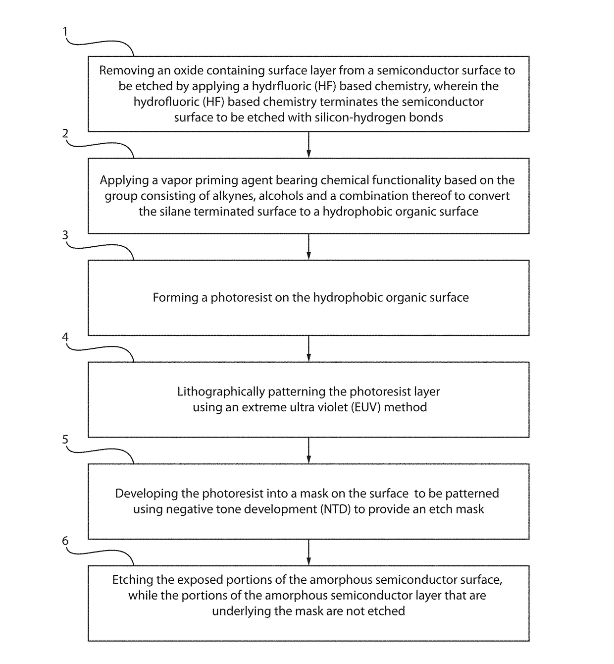
[0024]Principles and embodiments of the present invention relate generally to fabricating microelectronics structures, and the resulting structures formed thereby, using extreme ultraviolet (EUV) lithographic and electron beam (E-beam) processes. Patterning of small features generated by extreme ultraviolet (EUV) and E-beam lithography can be limited by a variety of factors, from the photoresist over the substrate to the developer.

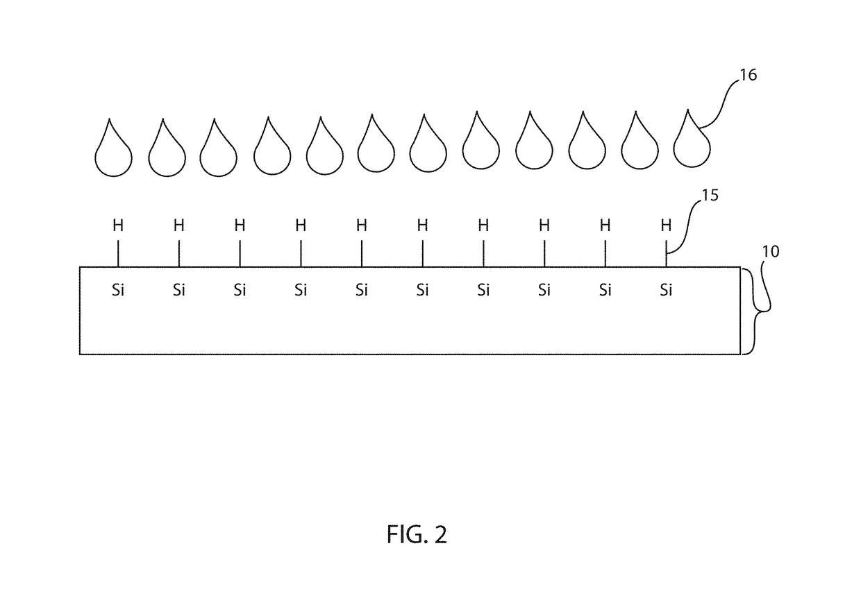
[0025]The methods and structures described herein provide for improved adhesion promotion for photoresist material layers used in EUV and R-beam lithography. In some embodiments, the method includes stripping the top surface oxide layer, e.g., silicon oxide (SiOx) layer, from a silicon containing layer, or other type IV semiconductor surface, with a hydrofluoric containing chemistry, such as diluted hydrofluoric acid (dHF), to generate a silane (SiH) terminated silicon surface and delivering a vapor priming agent bearing chemical functionality based on alk...


PUM


Abstract

An etch process that includes removing an oxide containing surface layer from a semiconductor surface to be etched by applying a hydrofluoric (HF) based chemistry, wherein the hydrofluoric (HF) based chemistry terminates the semiconductor surface to be etched with silicon-hydrogen bonds, and applying a vapor priming agent bearing chemical functionality based on the group consisting of alkynes, alcohols and a combination thereof to convert the silane terminated surface to a hydrophobic organic surface. The method continues with forming a photoresist layer on the hydrophobic organic surface; and patterning the photoresist layer. Thereafter, the patterned portions of the photoresist are developed to provide an etch mask. The portions of the semiconductor surface exposed by the etch mask are then etched.

Description

BACKGROUNDTechnical Field[0001]The present invention generally relates to lithographic materials for extreme ultraviolet (EUV) and electron beam (E-beam) lithography, and more particularly to inorganic hardmask processing used in EUV lithography.Description of the Related Art[0002]Semiconductor fabrication typically involves transfer of a pattern from a mask to a resist using lithography, and transfer of the pattern from the resist to a hardmask through etching. The pattern can then be transferred from the hardmask to a semiconductor material through further etching processes. In general, photolithography (in contrast to e-beam lithography, for example) uses light to form an image of the mask on a photoresist material, where the incident light can cause a photo reaction. Light for photolithography has progressed from wavelengths in the range of 436 nm (blue light) to 365 nm (near ultraviolet (UV)) to 248 nm (deep UV) to a wavelength of 193 nm. The wavelength of light has moved to sm...

Claims


Application Information

Patent Timeline
IPC IPC(8): H01L21/033G03F7/20H01L21/027
CPCH01L21/0338H01L21/0337H01L21/0335H01L21/0332H01L21/0274G03F7/70033G03F7/70016G03F7/16G03F7/0751
Inventor GLODDE, MARTINGOLDFARB, DARIO L.
Owner IBM CORP
Why Eureka
Try Eureka