Hybrid photonic non-blocking wide spectrum WDM on-chip router

a wide spectrum, on-chip router technology, applied in optics, instruments, electrical equipment, etc., can solve the problems of delay and power dissipation, clamping performance, and performance bottlenecks of electronic devices, so as to improve system performance, improve photonic integrated routing performance, and save energy consumption

Active Publication Date: 2018-08-30
GEORGE WASHINGTON UNIVERSITY
View PDF2 Cites 6 Cited by
  • Summary
  • Abstract
  • Description
  • Claims
  • Application Information

AI Technical Summary

Benefits of technology

[0007]To address these and other deficiencies in the art, disclosed herein is an optical router design using a hybrid plasmonic-photon approach and emerging unity-high index tuning materials simultaneously to improve photonic integrated routing performance in all three factors. The enabling technological insights are based on the strong index tunability of the underlying optical plasmonic hybrid mode enabling short 2×2 switches based on voltage-controlled directional-couplers. Cascading a network of these plasmonic 2×2 switches can be used to design a compact optical router since the switching length scales inversely with index-...

Problems solved by technology

However, physical limitations such as power and thermal budget constraints appose these demands restricted by technology densification as seen in multicore technology and simple I/O capacity [2].
However, the majority of optical network-on-chip (NoC) routers perform their role not exclusively in the photonic domain but often in capacitive-limiting electronics.
Yet, the known performance bottlenecks of electronic devices, namely mainly delay and power dissipation, and clamping performance.
Turning to optical routing, on the other hand, is in itself inefficient given the current photonics technology due to the low light...

Method used


Image

  • Hybrid photonic non-blocking wide spectrum WDM on-chip router
  • Hybrid photonic non-blocking wide spectrum WDM on-chip router
  • Hybrid photonic non-blocking wide spectrum WDM on-chip router

Examples


Embodiment Construction

[0016]In describing the illustrative, non-limiting preferred embodiments of the invention illustrated in the drawings, specific terminology will be resorted to for the sake of clarity. However, the invention is not intended to be limited to the specific terms so selected, and it is to be understood that each specific term includes all technical equivalents that operate in similar manner to accomplish a similar purpose. Several preferred embodiments of the invention are described for illustrative purposes, it being understood that the invention may be embodied in other forms not specifically shown in the drawings.

[0017]The present invention is a hybrid photonic-plasmonic broadband switch design. One illustrative non-limiting embodiment of the invention is shown in the figures and described below.

Technology Hybridization

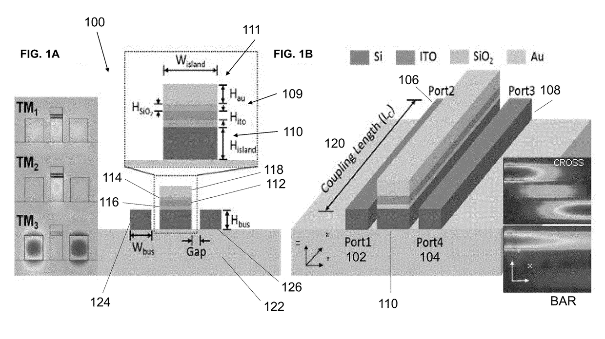
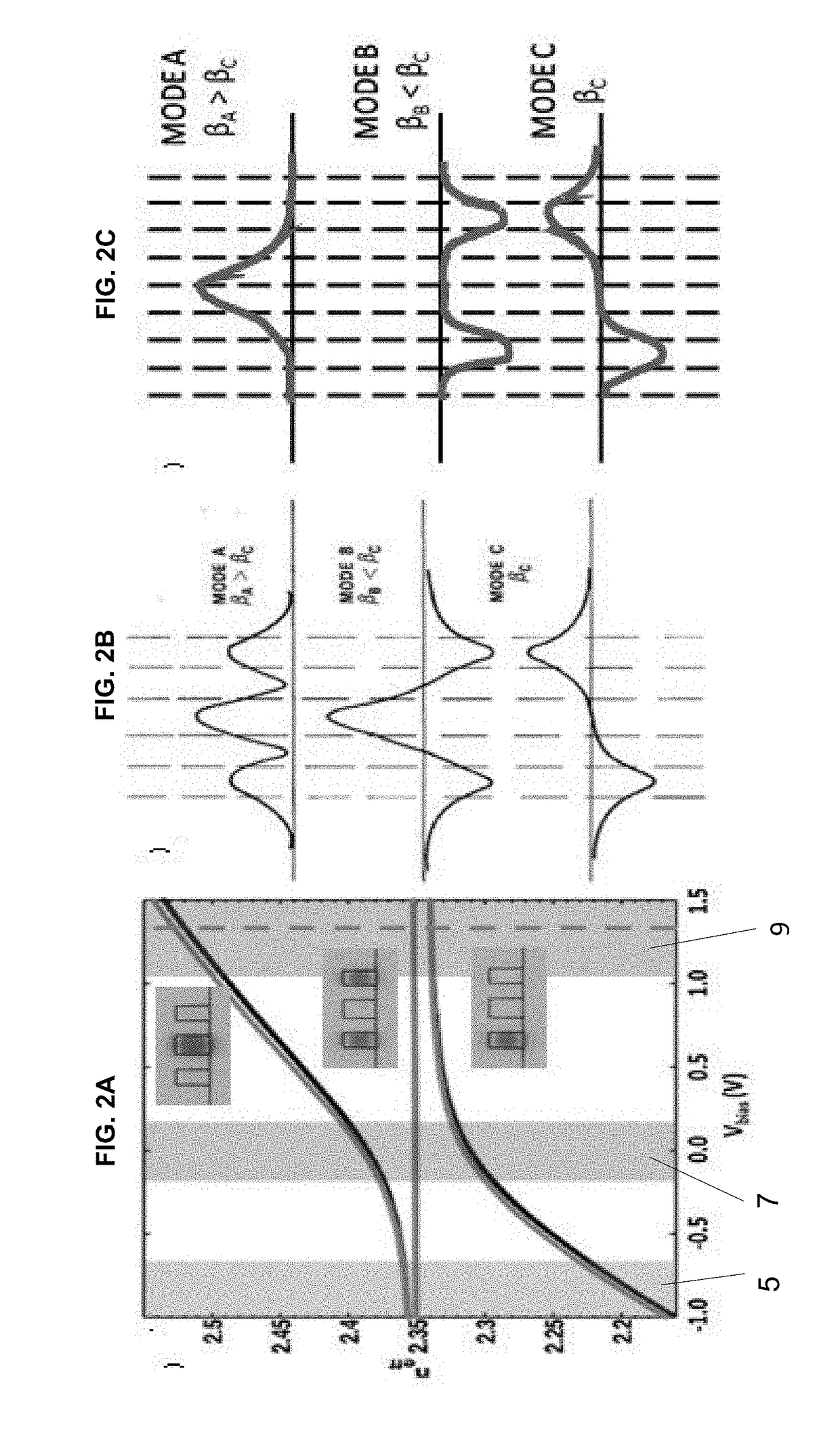
[0018]The fundamental building block of the optical router is a 2×2 optical switch, namely a voltage-controlled directional coupler whose performance directly impacts ...


PUM


Abstract

Photonic data routing in optical networks is expected overcome the limitations of electronic routers with respect to data rate, latency, and energy consumption. However photonics-based routers suffer from dynamic power consumption, and non-simultaneous usage of multiple wavelength channels when microrings are deployed and are sizable in footprint. Here we show a design for the first hybrid photonic-plasmonic, non-blocking, broadband 5×5 router based on 3-waveguide silicon photonic-plasmonic 2×2 switches. The compactness of the router (footprint <200 μm2) results in a short optical propagation delay (0.4 ps) enabling high data capacity up to 2 Tbps. The router has an average energy consumption ranging from 0.1˜1.0 fJ/bit depending on either DWDM or CDWM operation, enabled by the low electrical capacitance of the switch. The total average routing insertion loss of 2.5 dB is supported via an optical mode hybridization deployed inside the 2×2 switches, which minimizes the coupling losses between the photonic and plasmonic sections of the router. The router's spectral bandwidth resides in the S, C and L bands and exceeds 100 nm supporting WDM applications since no resonance feature are required. Moreover, this hybrid photonic-plasmonic switch design is also suitable for 3 up to a few dozens of routing ports by simply cascading our 2×2 switch with a specific pattern. Taken together this novel optical router combines multiple design features, all required in next generation high data-throughput optical networks and computing systems.

Description

RELATED APPLICATIONS[0001]This application claims the benefit of U.S. Provisional Application No. 62 / 454,208, filed Feb. 3, 2017, the entire contents of which are incorporated herein by reference.GOVERNMENT LICENSE RIGHTS[0002]This invention was made with government support under the Air Force Office of Scientific Research (AFOSR) award number FA9550-15-1-0447 which is part of the Dynamic Data-Driven Applications System (DDDAS) program, and by AFOSR award number FA9550-14-1-0378, and by AFOSR award number FA9550-17-P-0014 of the small business innovation research (SBIR) program. The government has certain rights in the invention.BACKGROUND OF THE INVENTIONField of the Invention[0003]The present invention relates to a silicon-based, broadband waveguide-integrated electro-optical switch for performing optical switching. More particularly, the present invention relates to an electro-optical switch for optically coupling and decoupling silicon-based waveguides.BACKGROUND OF THE RELATED ...

Claims


Application Information

Patent Timeline
IPC IPC(8): G02F1/313H04Q11/00
CPCG02F1/3132H04Q11/0005G02F2001/311H04Q2011/0039H04Q2011/0041H04Q2011/0007G02F1/311
Inventor SUN, SHUAISORGER, VOLKER J.EL-GHAZAWI, TAREKNARAYANA, VIKRAM K.
Owner GEORGE WASHINGTON UNIVERSITY
Why Eureka
Try Eureka