Semiconductor device

a technology of semiconductor devices and insulating films, applied in the direction of semiconductor devices, basic electric elements, electrical apparatus, etc., can solve the problems of insufficient technique for relaxing electric field concentration, and inability to function as mosfets, etc., to reduce the distance between the protective diffusion layer grounding region and the protective diffusion layer at the bottom of each trench, reduce the effect of gate insulating film breakage caused by current crowding in a trans

Active Publication Date: 2018-08-30
MITSUBISHI ELECTRIC CORP
View PDF2 Cites 4 Cited by
  • Summary
  • Abstract
  • Description
  • Claims
  • Application Information

AI Technical Summary

Benefits of technology

[0019]According to the present invention, the striped active regions through which a main current conducts and the striped contact regions which have the protective-diffusion-layer grounding regions are alternately disposed; thereby, variations in distance from the protective-diffusion-layer grounding region to the protective diffusion layer at the bottom of each of the trenches are reduced. Thus, the breakage of the gate insulating film caused by current crowding in a transient response can be reduced. Further, according to the present invention, the second side surface of the striped gate electrode is covered with a thickness larger than that of the gate insulating film. Consequently, the capacitance between the source electrode and the second side surface of the striped gate electrode facing the source electrode is reduced. Thus, the switching speed can be increased.
[0020]The object, features, aspects, and advantages of the present invention will become more apparent from the following detailed description and the accompanying drawings.

Problems solved by technology

However, the trench-gate MOSFETs for controlling power have a problem with a gate oxide film susceptible to breakage due to the electric field concentration at the bottom of trenches.
When the gate oxide film breaks down, the element fails to function as an MOSFET.
This technique is effective at relaxing the electric field concentration but is insufficient from the viewpoint of its switching.
Since this time is longer than the switching time, simply disposing the protective diffusion layer does not allow for sufficiently high switching speed.
Thus, increase in the switching speed may be insufficient under this technique.

Method used


Image

  • Semiconductor device
  • Semiconductor device
  • Semiconductor device

Examples


embodiment 1

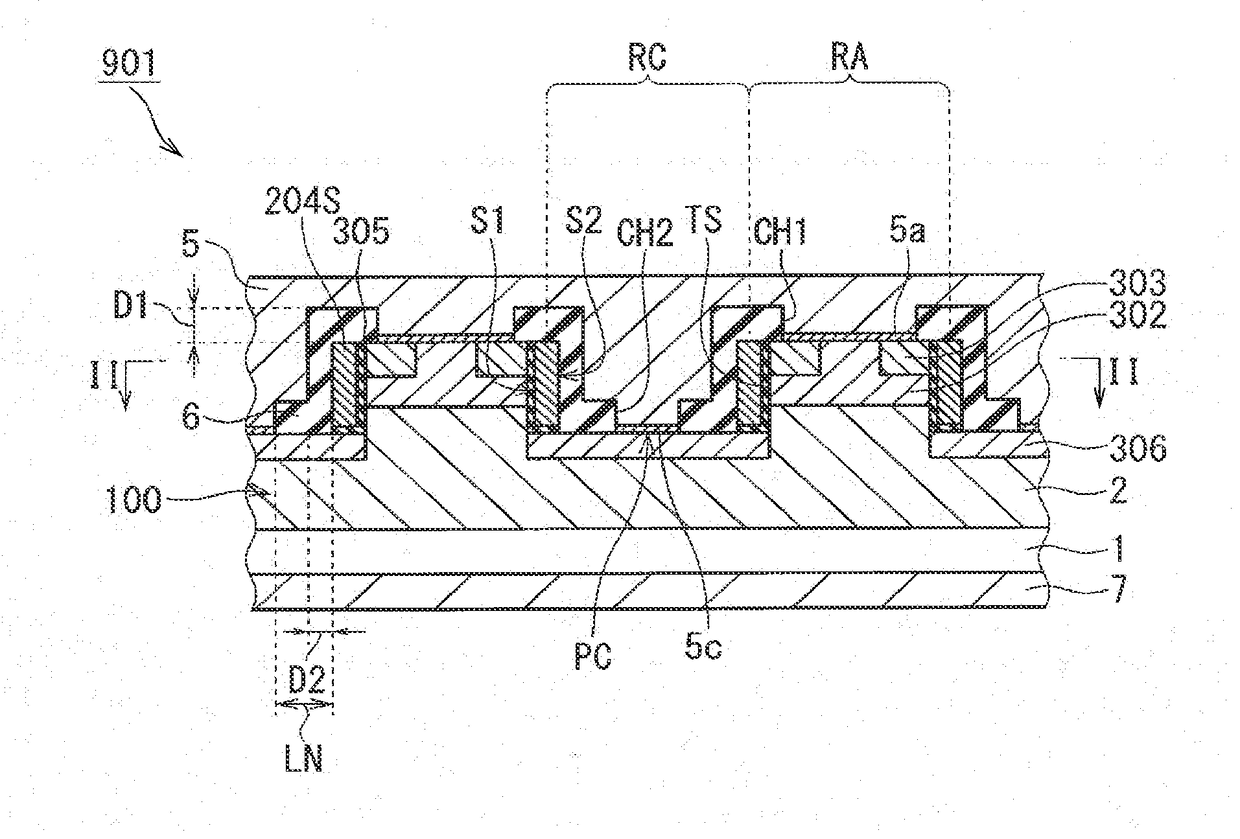
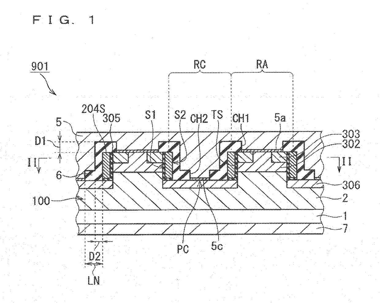
[0047]FIGS. 1 and 2 each is a partial sectional view schematically illustrating a structure of an MOSFET 901 (a semiconductor device) according to Embodiment 1. The field of view of FIG. 1 is shown along the line I-I of FIG. 2, and the field of view of FIG. 2 is shown along the line II-II of FIG. 1.

[0048]The MOSFET 901 includes, in a plan view (a field of view corresponding to FIG. 2, i.e., a field of view corresponding to a plane perpendicular to a thickness direction), a plurality of striped active regions RA extending in a longitudinal direction (a horizontal direction in FIG. 2) and a plurality of striped contact regions RC extending in the same longitudinal direction. A striped pattern provided with the MOSFET 901 by alternately and repeatedly disposing the striped active regions RA and the striped contact regions RC in a direction perpendicular to the longitudinal direction (a vertical direction in FIG. 2). The striped active regions RA are regions actually functioning as MOSF...

embodiment 2

[0104]FIGS. 16 and 17 each is a partial sectional view schematically illustrating a structure of an MOSFET 908 (a semiconductor device) according to Embodiment 2. The field of view of FIG. 16 is shown along the line XVI-XVI of FIG. 17, and the field of view of FIG. 17 is shown along the line XVII-XVII of FIG. 16. The field of view of FIG. 16 is the same as that of FIG. 2, and the field of view of FIG. 17 is the same as that of FIG. 1.

[0105]The MOSFET 908 further includes supporting regions 207 in addition to the structure of the MOSFET 901 (FIGS. 1 and 2). Each of the supporting regions 207 protrudes from the bottom of the striped trench TS and away from the source electrode 5 between the striped active region RA and the striped contact region RC. Thus, the supporting regions 207 are not connected to the source electrode 5; the supporting regions 207, therefore, do not have any electrical function. The supporting regions 207 each have a pair of side surfaces that are opposite to eac...

embodiment 3

[0116]FIGS. 18 and 19 each is a partial sectional view schematically illustrating a structure of an MOSFET 909 (a semiconductor device) according to Embodiment 3. The field of view of FIG. 18 is shown along the line XVIII-XVIII of FIG. 19, and the field of view of FIG. 19 is shown along the line XIX-XIX of FIG. 18. The field of view of FIG. 18 is the same as that of FIG. 2, and the field of view of FIG. 19 is the same as that of FIG. 1.

[0117]The MOSFET 909 differs from the MOSFET 901 only in the structure of the striped active regions RA. Specifically, the MOSFET 909 further includes intermediate trenches TM and intermediate gate electrodes 204M in addition to the structure of the MOSFET 901 (FIGS. 1 and 2). The intermediate trenches TM are formed between the two adjacent striped trenches TS. The intermediate trench TM penetrates the source region 303 and the base region 302 to reach the drift layer 2. The intermediate trenches TM are shallower than the striped trenches TS. The prot...


PUM


Abstract

A semiconductor device in which an interlayer insulation film covers striped gate electrodes with a thickness larger than a thickness of a gate oxide film. The interlayer insulation film includes first contact holes outside each striped trench, and second contact holes inside the striped trench. In a plan view, striped active regions and striped contact regions both extending in a longitudinal direction exist. The striped active regions and the striped contact regions are alternately and repeatedly disposed in a direction perpendicular to the longitudinal direction. In each of the striped active regions, the source electrode is connected to a source region through the first contact hole. In each of the striped contact regions, the source electrode is connected to a protective diffusion layer through the second contact hole.

Description

TECHNICAL FIELD[0001]The present invention relates to a semiconductor device, and particularly to a trench-gate power semiconductor device.BACKGROUND ART[0002]Insulated gate semiconductor devices such as ate insulated gate bipolar transistor (IGBT) and a metal oxide semiconductor field effect transistor (MOSFET) have been widely used in power electronics equipment as switching elements for controlling the power supplied to loads such as a motor. Power loss in the switching elements is preferably less in view of energy saving. Indicators representing g this loss include ON resistance. The ON resistance represents a drain-source electrical resistance when the MOSFET is turned ON. The switching elements suitable for reducing the ON resistance include trench-gate MOSFETs each with a gate electrode embedded in a semiconductor layer. The trench-gate MOSFETs can have channel width densities higher than those of normal planar MOSFETs. Thus, the ON resistance per unit area can be reduced.[00...

Claims


Application Information

Patent Timeline
Patent Type & Authority Applications(United States)
IPC IPC(8): H01L29/16H01L29/423H01L29/49H01L29/78H01L29/417
CPCH01L29/1608H01L29/42316H01L29/49H01L29/78H01L29/41725H01L29/41766H01L29/66068H01L29/417H01L29/45H01L29/7396H01L29/7397H01L29/0696H01L29/407H01L29/7813H01L29/0623
Inventor SUGAWARA, KATSUTOSHITANAKA, RINAFUKUI, YUTAKAADACHI, KOHEIKONISHI, KAZUYA
Owner MITSUBISHI ELECTRIC CORP
Why Eureka
Try Eureka