The greater the overlay error, the more the structures are misaligned.
If the overlay error is too great, the performance of the manufactured electronic device may be compromised.
Unfortunately, these specialized target structures often do not conform to the design rules of the particular semiconductor manufacturing process being employed to generate the electronic device.
This leads to errors in
estimation of overlay errors associated with actual device structures that are manufactured in accordance with the applicable design rules.
However, relying solely on
asymmetry as the indicator of overlay error is problematic because process induced variations, including both symmetric and asymmetric variations, significantly affect the overlay measurement.
This results in an inaccurate measurement of overlay error.
Unfortunately, both of these approaches are limited in their effectivity.
This makes the measurement unreliable and inconsistent, requiring frequent reevaluation of illumination
wavelength.
Target design optimization is very
time consuming and requires accurate models of the structures, material dispersions, and the optical system.
It is also very challenging to verify the accuracy of the models because the
mask and targets are typically not available at the time of
recipe development.
In addition, target optimization may reduce measurement sensitivity to process variations, but does not fully address robustness to the full window of process variations.
However, the presence of symmetric and asymmetric process variations causes shifts in the inaccuracy landscape which complicates the selection of a suitable illumination
wavelength.
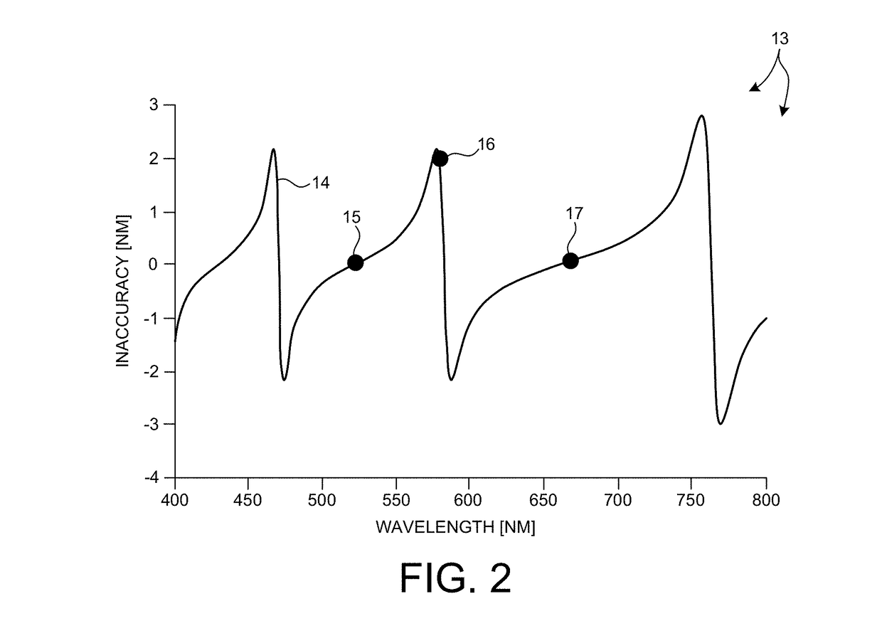
As illustrated in FIG. 3, as structural
asymmetry increases, for example, due to printing errors, the amplitude of the induced inaccuracy of the overlay measurement increases.
As a result, the selection of a suitable illumination wavelength based on a particular inaccuracy landscape may prove inadequate in the presence of asymmetric and symmetric process variations.
One may attempt to mitigate this risk by selecting the illumination wavelength in light of a number of inaccuracy landscapes that encompass a range of symmetric and asymmetric process variations, but in some examples, the variations may be so large that there is no illumination wavelength that will result in a sufficiently accurate overlay measurement.
As a result, in some cases, it is impossible to generate an overlay measurement
recipe based on the selection of illumination wavelength.
In addition, the overlay accuracy of conventional SCOL and DBO techniques is significantly affected by optical system variations and aberrations.
This makes it difficult to achieve accurate overlay measurements and sufficiently accurate tool matching.
Future overlay metrology applications present challenges for metrology due to increasingly small resolution requirements and the increasingly high value of
wafer area.

