
Process robust overlay metrology based on optical scatterometry

a technology of optical scatterometry and overlay measurement, applied in the field ofmetrology systems and methods, can solve the problems of specialized target structures not meeting design rules, more structures are misaligned, and the performance of manufactured electronic devices may be compromised

Active Publication Date: 2020-08-04
KLA CORP
View PDF59 Cites 0 Cited by
  • Summary
  • Abstract
  • Description
  • Claims
  • Application Information

AI Technical Summary

Benefits of technology

The patent text describes a method to improve the accuracy of measuring semiconductor device parameters by collecting scattered light data from multiple targets with different structures and using different measurement techniques. This approach increases the amount of information and reduces the correlation between different measurements, resulting in more accurate models and improved reliability.

Problems solved by technology

The greater the overlay error, the more the structures are misaligned.
If the overlay error is too great, the performance of the manufactured electronic device may be compromised.
Unfortunately, these specialized target structures often do not conform to the design rules of the particular semiconductor manufacturing process being employed to generate the electronic device.
This leads to errors in estimation of overlay errors associated with actual device structures that are manufactured in accordance with the applicable design rules.
However, relying solely on asymmetry as the indicator of overlay error is problematic because process induced variations, including both symmetric and asymmetric variations, significantly affect the overlay measurement.
This results in an inaccurate measurement of overlay error.
Unfortunately, both of these approaches are limited in their effectivity.
For example, the selection of a specific illumination wavelength may result in small overlay measurement errors, but only within a small range of the full process window.
This makes the measurement unreliable and inconsistent, requiring frequent reevaluation of illumination wavelength.
Target design optimization is very time consuming and requires accurate models of the structures, material dispersions, and the optical system.
It is also very challenging to verify the accuracy of the models because the mask and targets are typically not available at the time of recipe development.
In addition, target optimization may reduce measurement sensitivity to process variations, but does not fully address robustness to the full window of process variations.
However, the presence of symmetric and asymmetric process variations causes shifts in the inaccuracy landscape which complicates the selection of a suitable illumination wavelength.
As illustrated in FIG. 3, as structural asymmetry increases, for example, due to printing errors, the amplitude of the induced inaccuracy of the overlay measurement increases.
As a result, the selection of a suitable illumination wavelength based on a particular inaccuracy landscape may prove inadequate in the presence of asymmetric and symmetric process variations.
One may attempt to mitigate this risk by selecting the illumination wavelength in light of a number of inaccuracy landscapes that encompass a range of symmetric and asymmetric process variations, but in some examples, the variations may be so large that there is no illumination wavelength that will result in a sufficiently accurate overlay measurement.
As a result, in some cases, it is impossible to generate an overlay measurement recipe based on the selection of illumination wavelength.
In addition, the overlay accuracy of conventional SCOL and DBO techniques is significantly affected by optical system variations and aberrations.
This makes it difficult to achieve accurate overlay measurements and sufficiently accurate tool matching.
Future overlay metrology applications present challenges for metrology due to increasingly small resolution requirements and the increasingly high value of wafer area.

Method used


Image

  • Process robust overlay metrology based on optical scatterometry
  • Process robust overlay metrology based on optical scatterometry
  • Process robust overlay metrology based on optical scatterometry

Examples


Embodiment Construction

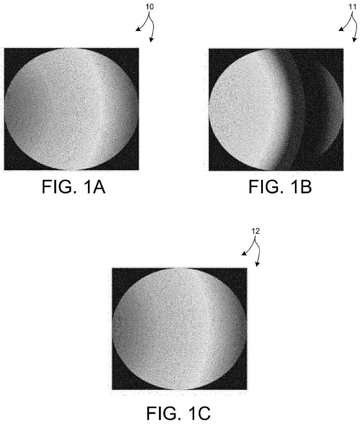
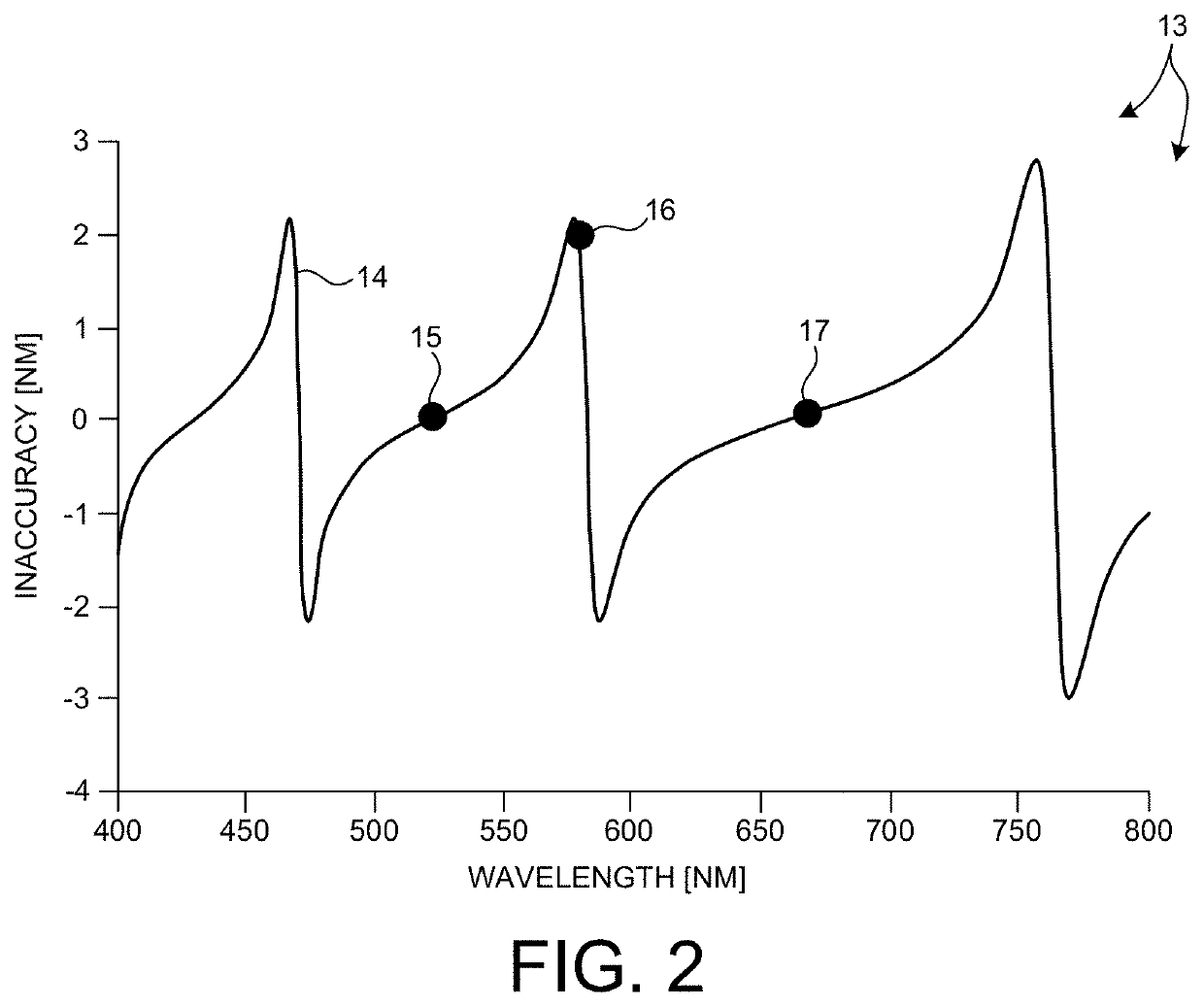
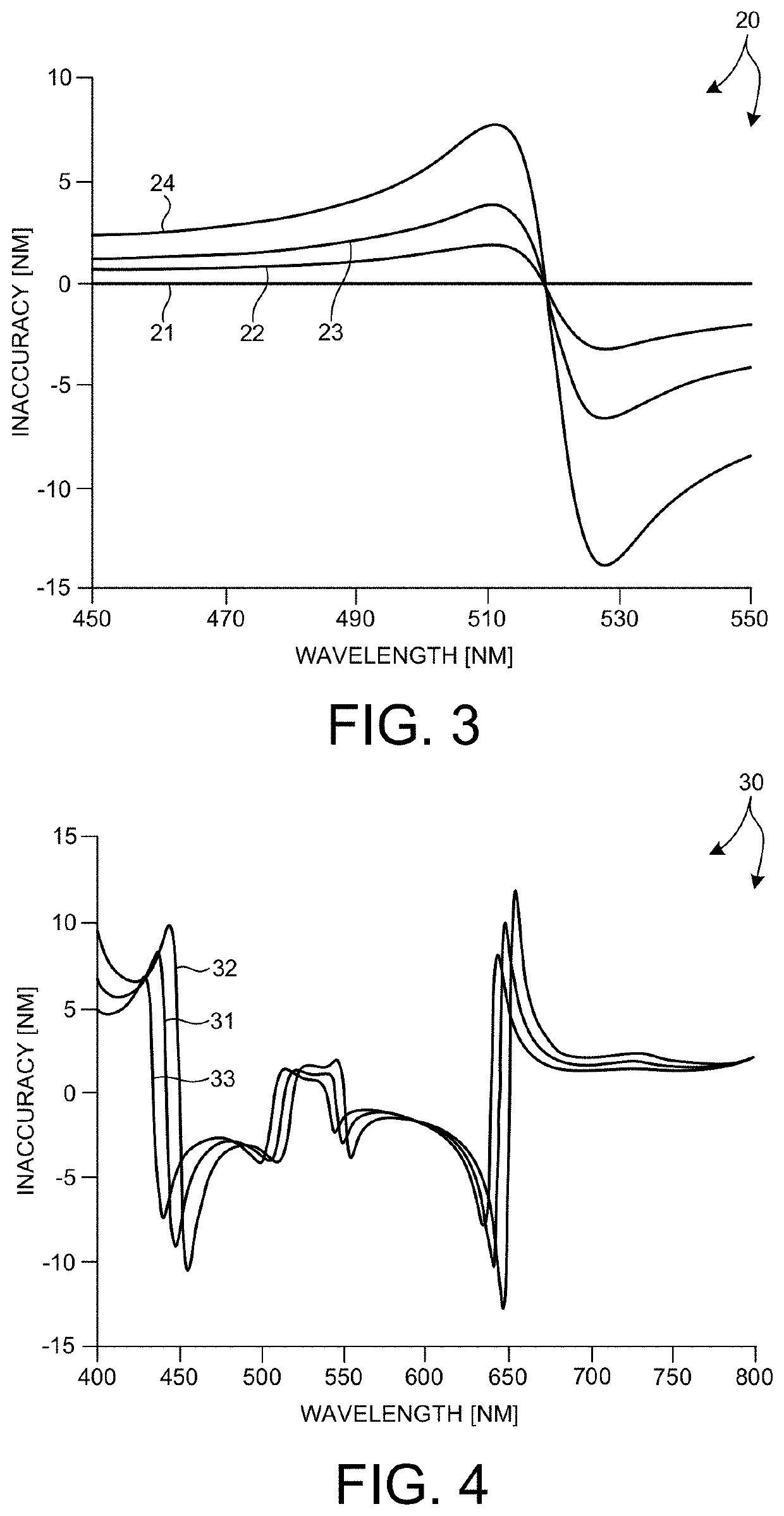
[0051]Reference will now be made in detail to background examples and some embodiments of the invention, examples of which are illustrated in the accompanying drawings.

[0052]Methods and systems for robust overlay error measurement based on a trained measurement model are described herein. The measurement model is trained from raw scatterometry data collected from Design of Experiments (DOE) wafers by a scatterometry based overlay metrology system. Each measurement site includes one or more metrology targets fabricated with programmed overlay variations and known process variations. Each measurement site is measured with known metrology system variations (i.e., measurement system parameter values) to which the scatterometry based overlay metrology system is sensitive. In this manner, the measurement model is trained to separate actual overlay from process variations and metrology system variations which affect the overlay measurement. Thus, an estimate of actual overlay by the traine...


PUM

PropertyMeasurementUnit
illumination wavelengthaaaaaaaaaa

Abstract

Methods and systems for robust overlay error measurement based on a trained measurement model are described herein. The measurement model is trained from raw scatterometry data collected from Design of Experiments (DOE) wafers by a scatterometry based overlay metrology system. Each measurement site includes one or more metrology targets fabricated with programmed overlay variations and known process variations. Each measurement site is measured with known metrology system variations. In this manner, the measurement model is trained to separate actual overlay from process variations and metrology system variations which affect the overlay measurement. As a result, an estimate of actual overlay by the trained measurement model is robust to process variations and metrology system variations. The measurement model is trained based on scatterometry data collected from the same metrology system used to perform measurements. Thus, the measurement model is not sensitive to systematic errors, aysmmetries, etc.

Description

CROSS REFERENCE TO RELATED APPLICATION[0001]The present application for patent claims priority under 35 U.S.C. § 119 from U.S. provisional patent application Ser. No. 62 / 465,163, entitled “Method and System for Process-Robust Overlay Metrology Using Optical Scatterometry,” filed Mar. 1, 2017, the subject matter of which is incorporated herein by reference in its entirety.TECHNICAL FIELD[0002]The described embodiments relate to metrology systems and methods, and more particularly to methods and systems for improved overlay measurement.BACKGROUND INFORMATION[0003]Semiconductor devices such as logic and memory devices are typically fabricated by a sequence of processing steps applied to a specimen. The various features and multiple structural levels of the semiconductor devices are formed by these processing steps. For example, lithography among others is one semiconductor fabrication process that involves generating a pattern on a semiconductor wafer. Additional examples of semiconduc...

Claims


Application Information

Patent Timeline
Patent Type & Authority Patents(United States)
IPC IPC(8): G03F7/20G01B11/14
CPCG03F7/70616G03F7/70633G01B11/14G06T7/001G06T2207/10061G06T2207/20081G06T2207/20084G06T2207/30148G03F7/705G03F7/70425G06F2207/4824G06T7/60G06F7/4812G01N21/8851G01N21/47G01N21/9501
Inventor PANDEV, STILIAN IVANOVSHCHEGROV, ANDREI V.LU, WEI
Owner KLA CORP
Learn More