Photocatalyst electrode and artificial photosynthesis module

a photocatalyst and electrode technology, applied in the direction of electrolysis components, catalyst activation/preparation, physical/chemical process catalysts, etc., can solve the problems of limited reaction field and difficult to make the reaction efficiency per installation area of the electrode for optical water decomposition high, and achieve high reaction efficiency and stably generating gas over a long period of time.

Inactive Publication Date: 2018-10-11
FUJIFILM CORP +1
View PDF0 Cites 3 Cited by
  • Summary
  • Abstract
  • Description
  • Claims
  • Application Information

AI Technical Summary

Benefits of technology

[0012]According to the invention, the photocatalyst electrode and the artificial photosynthesis module with high reaction efficiency can be obtained. Additionally, the photocatalyst electrode and the artificial photosynthesis module capable of stably generating gas over a long period of time can be obtained.

Problems solved by technology

However, in JP2012-46385A, the reaction co-catalyst is laminated on the n-type semiconductor, a position where the reaction co-catalyst is provided is limited to the n-type semiconductor, and a reaction field is also limited.
In this case, it is difficult to make the reaction efficiency per installation area of the electrode for optical water decomposition high.
Moreover, it is also required to stably generate gas, such as hydrogen, over a long period of time.

Method used


Image

  • Photocatalyst electrode and artificial photosynthesis module
  • Photocatalyst electrode and artificial photosynthesis module
  • Photocatalyst electrode and artificial photosynthesis module

Examples


example 1

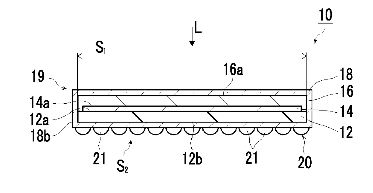
[0197]A soda lime glass substrate having a thickness of 1 mm was prepared as a substrate, and a molybdenum film having a thickness of 500 nm was formed on a surface of this soda lime glass substrate by the sputtering method to obtain a conductive layer. Next, a CIGS layer having a thickness of 1500 nm was formed as a p-type semiconductor layer on the conductive layer. Next, a CdS layer having a thickness of 50 nm was formed as an n-type semiconductor layer on the p-type semiconductor layer by the chemical bath deposition (CBD) method. A photocatalyst layer was formed of the p-type semiconductor layer and the n-type semiconductor layer. Hereinafter, the substrate in this state is referred to as a CIGS substrate. The CIGS substrate was cut into 1 cm×1 cm.

[0198]Next, Pt particles were made to be carried and supported with a set film thickness of 2 nm on the n-type semiconductor layer by the sputtering method to obtain an island-like second co-catalyst. Next, an indium tin oxide (ITO) l...

example 2

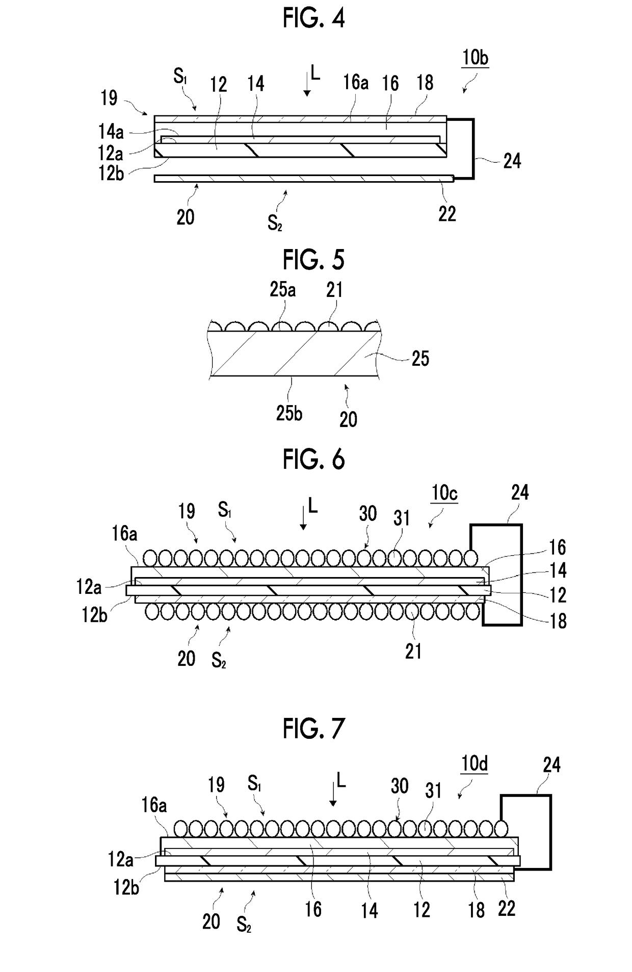
[0202]Since Example 2 is different from Example 1 in that a Pt film having a thickness of 50 nm was made as the first co-catalysts by the sputtering method, the second co-catalyst and the Pt film were electrically connected to each other with the conducting wire, the conducting wire was fixed using the conductive adhesive containing silver paste, was covered with the epoxy resin, and was electrically insulated from each other, and is the same as Example 1 excluding these, the detailed description thereof will be omitted.

[0203]In addition, the configuration of Example 2 is the same configuration as the photocatalyst electrode 10d illustrated in FIG. 7.

example 3

[0204]Since Example 3 is different from Example 1 in that a Pt mesh having an area 3 times greater than the area of the p-type semiconductor layer, that is, the photocatalyst layer was used as the first co-catalysts by the sputtering method, the second co-catalyst and the Pt mesh were electrically connected to each other with the conducting wire, the conducting wire was fixed using the conductive adhesive containing silver paste, was covered with the epoxy resin, and was electrically insulated from each other, and is the same as Example 1 excluding these, the detailed description thereof will be omitted. The installation area of Example 3 where a co-catalyst is provided is 4 times greater than the area of the photocatalyst layer.

[0205]In addition, the configuration of Example 3 is the same configuration as the photocatalyst electrode 10e illustrated in FIG. 8. A platinum mesh electrode that is made by EC Frontier CO., LTD. and has 80 meshes was used for the Pt mesh.


PUM

PropertyMeasurementUnit
light transmittanceaaaaaaaaaa

Abstract

A photocatalyst electrode decomposes water with light to generate gas. The photocatalyst electrode has a laminate including a substrate, a conductive layer provided on a surface of the substrate, and a photocatalyst layer provided on a surface of the conductive layer, and a first co-catalyst electrically connected to the photocatalyst layer. The light is incident from the surface side of the photocatalyst layer of the laminate, and in a case where a region where the light is incident on the surface of the photocatalyst layer and above the surface is defined as a first region and the region other than the first region is defined as a second region, the first co-catalyst is provided at least in the second region. The first co-catalyst and the photocatalyst layer are electrically connected to each other by at least one of a transparent conductive layer provided on the surface of the photocatalyst layer or a wiring line.

Description

CROSS-REFERENCE TO RELATED APPLICATIONS[0001]This application is a Continuation of PCT International Application No. PCT / JP2016 / 080599 filed on Oct. 14, 2016, which claims priority under 35 U.S.C. § 119(a) to Japanese Patent Application No. 2015-249499 filed on Dec. 22, 2015. The above application is hereby expressly incorporated by reference, in its entirety, into the present application.BACKGROUND OF THE INVENTION1. Field of the Invention[0002]The present invention relates to a photocatalyst electrode that includes a photocatalyst layer and a co-catalyst and decomposes water with light to generate gas, and an artificial photosynthesis module using the photocatalyst electrode, and particularly, to a photocatalyst electrode and an artificial photosynthesis module in which the co-catalyst is provided in a region that does not hinder light incident on the photocatalyst layer.2. Description of the Related Art[0003]Nowadays, water is decomposed using a photocatalyst to obtain gases, suc...

Claims


Application Information

Patent Timeline
Patent Type & Authority Applications(United States)
IPC IPC(8): B01J27/045B01J35/02C01B3/04C25B1/04C25B9/16C25B11/04H01L31/0216
CPCB01J27/045B01J35/02C01B3/04C25B1/04C25B9/16C25B11/04H01L31/02161B01J27/0515B01J35/004B01J37/0238B01J37/0244B01J37/343B01J37/347B01J37/348C01B3/042C25B9/00C25B1/55H01L31/02167H01L31/022425H01L31/0481Y02E10/50Y02E60/36C25B9/40
Inventor KOBAYASHI, HIROYUKI
Owner FUJIFILM CORP
Why Eureka
Try Eureka