Energy controller for excimer-laser silicon crystallization

Active Publication Date: 2018-12-06
COHERENT LASERSYST
View PDF1 Cites 2 Cited by
  • Summary
  • Abstract
  • Description
  • Claims
  • Application Information

AI Technical Summary

Benefits of technology

The present invention is about a device for making a layer of silicon crystal on a surface. It works by giving many laser pulses to the silicon layer while moving the surface with respect to the laser pulses. The laser pulses have a flat-topped intensity profile and a certain width in the direction of the surface movement. The device includes a laser-emitter to generate and deliver the laser pulses, optics to make them flat-topped and deliver them to the surface, an electricity generator to power the laser-emitter, an energy monitor to measure the energy of the laser pulses, a control circuit with a digital filter to adjust the energy of the laser pulses to a preferred level, and a translating mechanism to move the surface with respect to the laser pulses. The device ensures a consistent energy level and minimizes energy fluctuations, which leads to improved quality of the silicon crystal layer.

Problems solved by technology

The process is a delicate one.

Method used


Image

  • Energy controller for excimer-laser silicon crystallization
  • Energy controller for excimer-laser silicon crystallization
  • Energy controller for excimer-laser silicon crystallization

Examples


Embodiment Construction

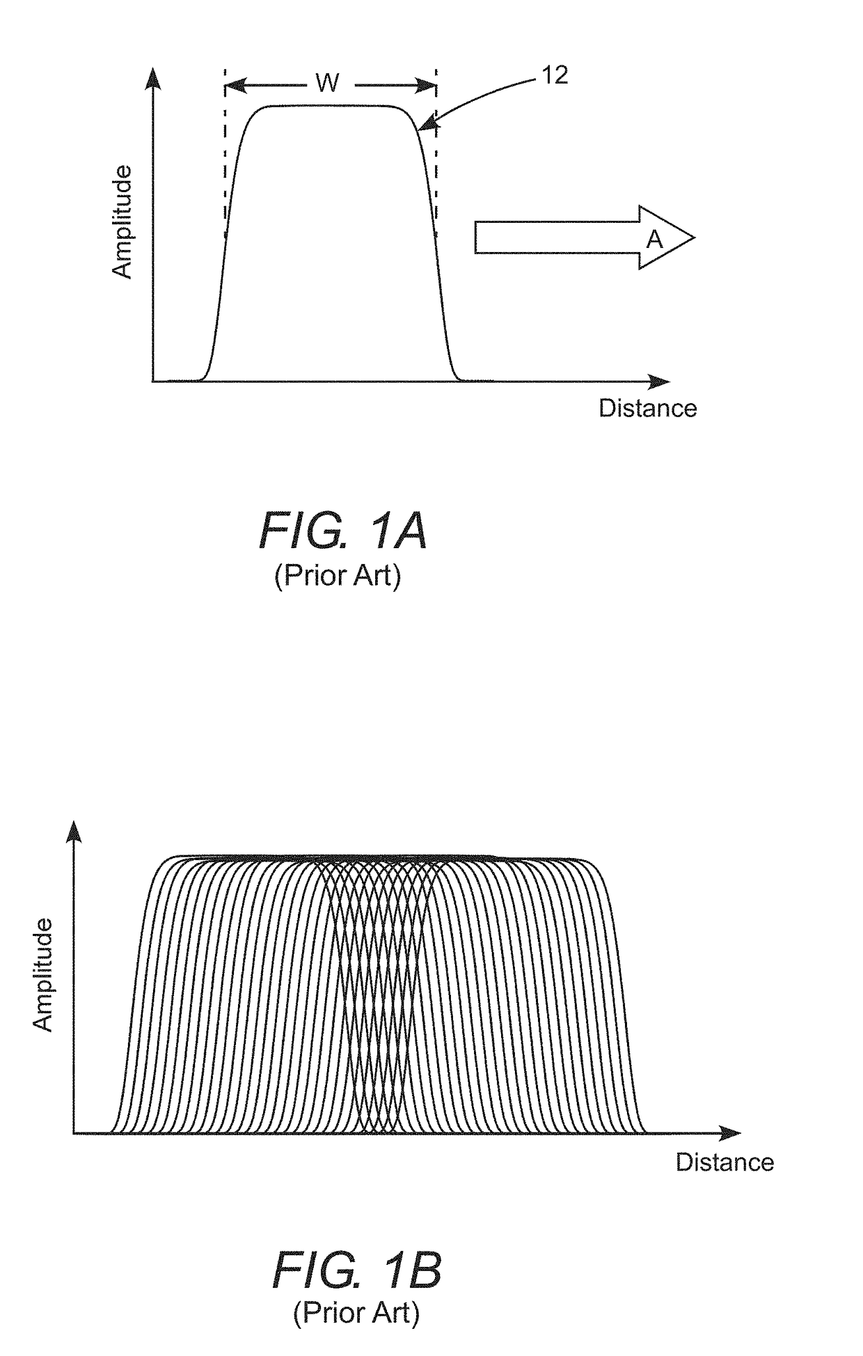
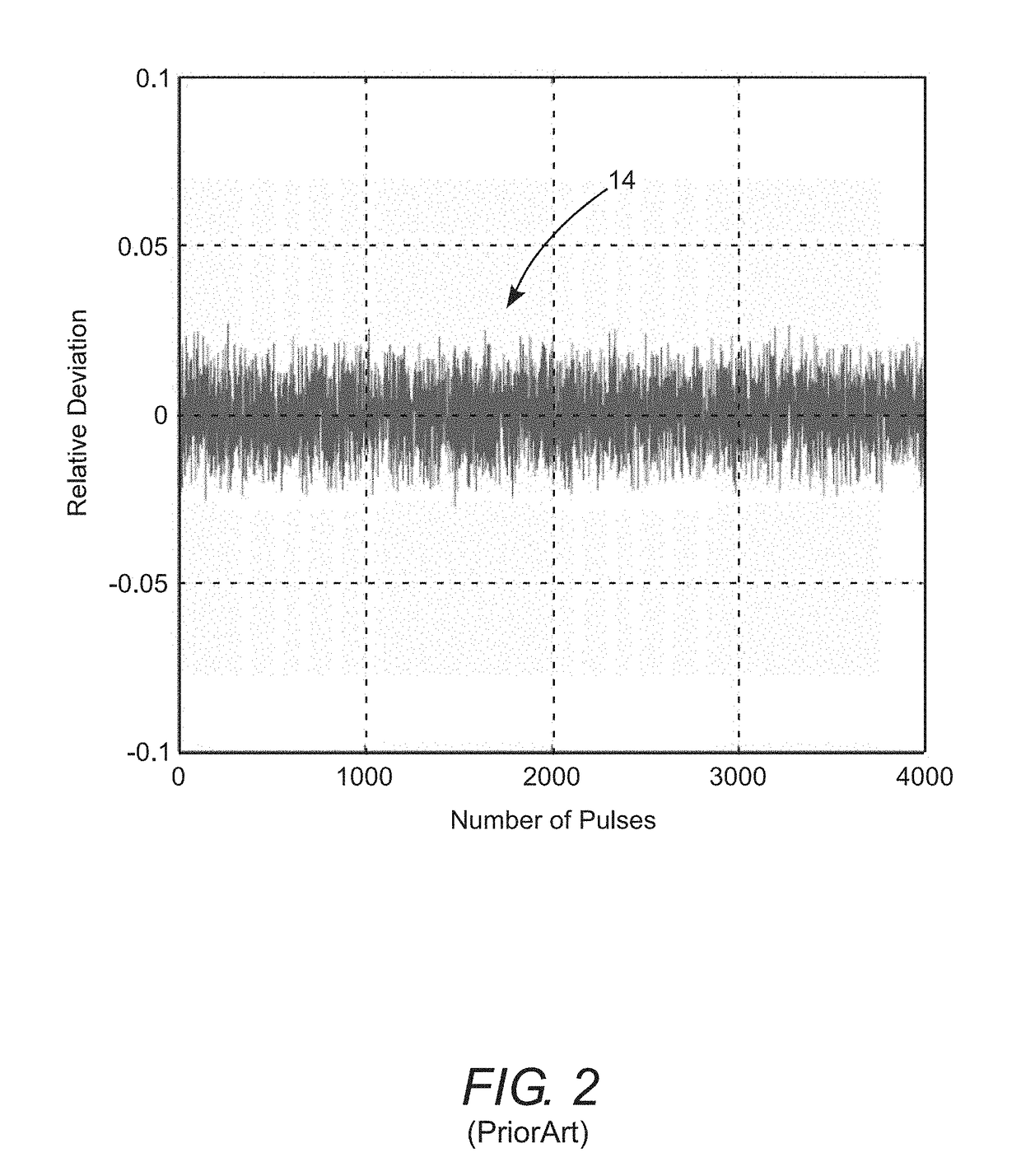
[0022]In arriving at the method and apparatus of the present invention, an analysis of prior-art energy control of excimer-laser output was performed. The analysis was performed for a plurality of laser pulses having the profile of FIG. 1A and consecutive laser pulses delivered in the overlapping manner of FIG. 1B. In particular, the effect of such laser-energy control on the stability of the radiation dosage applied to an above-discussed translated silicon layer was performed. A detailed description of this analysis is set forth below with reference to FIG. 2, FIG. 3, FIG. 4, and FIG. 5.

[0023]FIG. 2 is a graph schematically illustrating relative deviation of laser pulse-energy from a desired pulse-energy as a function of pulse-number (curve 14) for a hypothetical excimer laser controlled by prior-art methods. The graph was generated mathematically using a random-number generator to simulate pulse-to-pulse energy deviations such that the frequency spectrum of deviations has constant...


PUM


Abstract

Excimer laser annealing apparatus includes and excimer laser delivering laser-radiation pulses to a silicon layer supported on a substrate translated with respect to the laser pulses such that the consecutive pulses overlap on the substrate. The energy of each of the laser-radiation pulses is monitored, transmitted to control-electronics, and the energy of a next laser pulse is adjusted by a high-pass digital filter.

Description

TECHNICAL FIELD OF THE INVENTION[0001]The present invention relates in general to crystallization of a silicon layer using an excimer-laser beam. The invention relates in particular to repeated melting and crystallization of a silicon layer, by controlled irradiation with consecutive excimer-laser pulses.DISCUSSION OF BACKGROUND ART[0002]Flat panel displays are an enabling technology for all contemporary portable consumer electronic devices and large-format televisions. Silicon crystallization is a processing step that is often used in the manufacture of thin-film transistor (TFT) active-matrix liquid-crystal displays (AMLCDs) and active-matrix organic light-emitting diode (AMOLED) displays. Crystalline silicon forms a semiconductor base, in which electronic circuits of the display are formed by conventional lithographic processes.[0003]Commonly, crystallization is performed using a pulsed beam of laser-radiation that is shaped into the form of a long line having a uniform intensity...

Claims


Application Information

Patent Timeline
IPC IPC(8): G03F7/20H01S3/134H01S3/225H01S3/03H01S3/038
CPCG03F7/70025H01S3/134H01S3/225H01S3/038G03F7/70216G03F7/70041H01S3/03G03F7/70558H01L21/02532H01L21/02678H01L21/02686H01L21/02691H01S3/1305H01S3/1306
Inventor BRAGIN, IGOR
Owner COHERENT LASERSYST
Why Eureka
Try Eureka