Optical semiconductor device, optical subassembly, and optical module

a technology of optical subassembly and optical semiconductor, applied in the direction of semiconductor lasers, semiconductor laser structural details, instruments, etc., can solve the problems of deteriorating manufacturing yield, low amount of dopant material to be supplied, and precise control, so as to reduce the variation in supply of dopant material and cost

Active Publication Date: 2018-12-20
LUMENTUM JAPAN INC
View PDF0 Cites 2 Cited by
  • Summary
  • Abstract
  • Description
  • Claims
  • Application Information

AI Technical Summary

Benefits of technology

[0019]The present invention provides an optical semiconductor device, an optical subassembly, and an opt...

Problems solved by technology

Variation in diffusion of p-type dopant from the p-type semiconductor layer or the like toward the active layer affects the device characteristics and reliability of the semiconductor laser devices, which deteriorates the manufacturing yield.
The amount of dopant material to be supplied is very small and vulnera...

Method used


Image

  • Optical semiconductor device, optical subassembly, and optical module
  • Optical semiconductor device, optical subassembly, and optical module
  • Optical semiconductor device, optical subassembly, and optical module

Examples


first embodiment

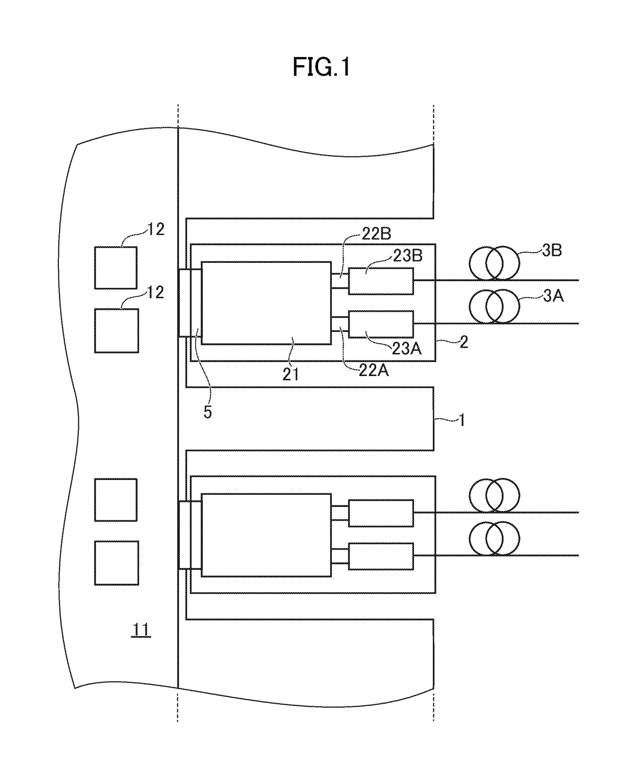
[0029]FIG. 1 is a schematic view of the structure of an optical transmission equipment 1 and optical modules 2 according to a first embodiment of the present invention. The optical transmission equipment 1 has a printed circuit board (PCB) 11 and an integrated circuit (IC) 12. The optical transmission equipment 1 is, for example, a large capacitor router or switch. The optical transmission equipment 1 has, for example, a function as an exchanger and is disposed in a base station or the like. The optical transmission equipment 1 has a plurality of optical modules 2 and receives data (a reception electric signal) from the optical module 2, determines which data is to be sent to where, using the IC 12 or the like, generates data for transmission (a transmission electric signal), and sends the data to a relevant optical module 2 via the printed circuit board 11.

[0030]The optical module 2 is a transceiver having a transmission function and a receiving function. The optical module 2 inclu...

second embodiment

[0081]An EA modulator integrated semiconductor laser device 200 according to the second embodiment of the present invention is an optical semiconductor device including a laser unit 200A, a modulator unit 200B, and a light waveguide portion 200C, all being monolithically integrated on a semiconductor substrate, in which the laser unit 200A is a Distributed Feedback (DFB) semiconductor laser device, and the modulator unit 200B is an EA modulator. The EA modulator integrated semiconductor laser device 200 according to this embodiment has a buried-hetero structure.

[0082]FIG. 7 is a bird-eye's view of the EA modulator integrated semiconductor laser device 200 according to this embodiment. The main characteristic of the EA modulator integrated semiconductor laser device 200 according to this embodiment lies in the structure of the p-type clad layer, similar to the first embodiment, in which the p-type clad layer includes one pair of a p-type InP layer and a p-type InAlP layer.

[0083]In th...

third embodiment

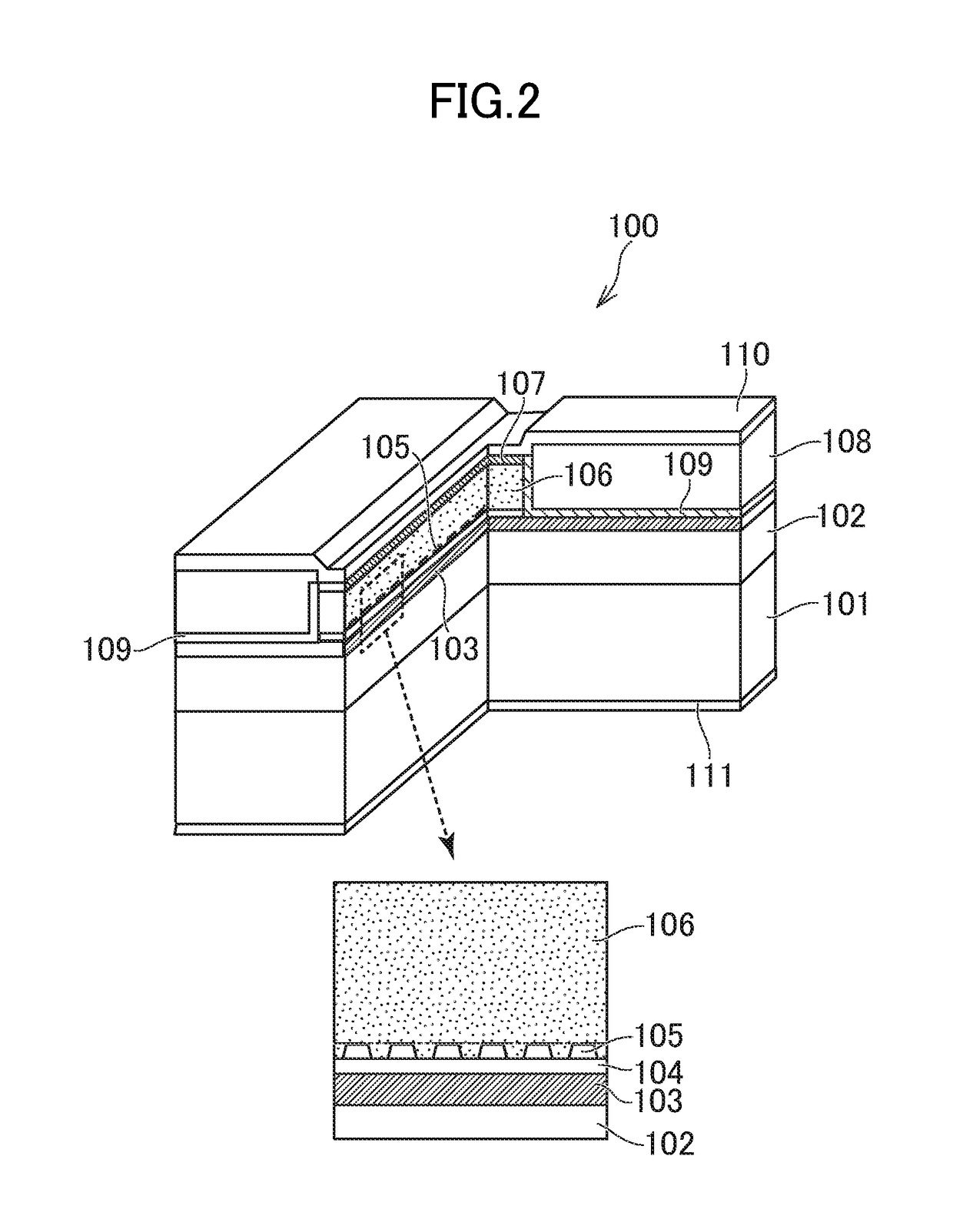
[0092]FIG. 8 is a cross sectional view of a PIN-type diode 300 according to a third embodiment of the present invention. A PIN-type diode according to this embodiment is an optical semiconductor device that is a semiconductor light-receiving element, whereas the optical semiconductor devices according to the first and second embodiments are semiconductor light-emitting elements. The main characteristic of the PIN-type diode 300 according to this embodiment lies in the structure of the p-type clad layer, similar to the first and second embodiment, in which the p-type clad layer includes three pairs of p-type InP layers and p-type InAlP layers.

[0093]Semiconductor multilayers including an n-type InGaAs contact layer 302, an n-type InP clad layer 303, an n-type InGaAsP SCH layer 304, an intrinsic InGaAs light absorbing layer 305, a p-type InGaAsP light absorbing layer 306, a p-type clad layer 307, and a p+-type InGaAs contact layer 308 are formed on a semi-insulating InP substrate 301. ...


PUM


Abstract

An optical semiconductor device includes an InP substrate; an active layer disposed above the InP substrate; a n-type semiconductor layer disposed below the active layer; and a p-type clad layer disposed above the active layer, wherein the p-type clad layer includes one or more p-type In1-xAlxP layers, the Al composition x of each of the one or more p-type In1-xAlxP layers is equal to or greater than a value corresponding to the doping concentration of a p-type dopant, and the absolute value of the average strain amount of the whole of the p-type clad layer is equal to or less than the absolute value of a critical strain amount obtained by Matthews' relational expression, using the entire layer thickness of the whole of the p-type clad layer as a critical layer thickness.

Description

CROSS-REFERENCE TO RELATED APPLICATION[0001]The present application claims priority from Japanese application JP 2017-117176, filed on Jun. 14, 2017, the content of which is hereby incorporated by reference into this application.BACKGROUND OF THE INVENTION1. Field of the Invention[0002]The present invention relates to an optical semiconductor device, an optical subassembly, and an optical module, and, in particular, to a technique for preventing variation in doping concentration of dopant in a clad layer of an optical semiconductor device.2. Description of the Related Art[0003]An optical semiconductor device may employ a so-called PIN structure in which an intrinsic (undoped) Multiple Quantum Well (MQW) layer is sandwiched between a p-type semiconductor layer and an n-type semiconductor layer. In this structure, the p-type and n-type semiconductor layers contains p-type and n-type dopants, respectively, that are doped thereinto so that the p-type and n-type semiconductor layers exhi...

Claims


Application Information

Patent Timeline
IPC IPC(8): H01S5/30H01L31/105H01L31/0304H01L31/18H01S5/02H01S5/026H01S5/22H01S5/343H01S5/042H01S5/12
CPCH01S5/3054H01L31/105H01L31/03046H01L31/1844H01S5/0208H01S5/026H01S5/22H01S5/3432H01S5/0425H04B10/40G02F1/015H01L31/03042H01L33/305H01S5/323H01S5/12H01S5/0014H01S5/0265H01S5/3211H01S5/34306H01S2301/173H01S2301/176H01S2304/04H01L31/0352H01L31/036H01L31/107H01S5/34366H01S5/3063H01S5/3218H01S5/343H01S5/3072H01S5/305H01S5/3403H01S5/3201
Inventor KITATANI, TAKESHIOKAMOTO, KAORUNAKAHARA, KOUJI
Owner LUMENTUM JAPAN INC
Why Eureka
Try Eureka