

Top-emitting woled display device
a display device and top-emitting technology, applied in the field of display, can solve the problems of difficult to simultaneously emit white light with three peaks of red, green and blue, difficult to meet the requirements of the existing amoled screen manufacturing technology, and achieve the effect of simple manufacturing procedur
- Summary
- Abstract
- Description
- Claims
- Application Information
AI Technical Summary
Benefits of technology
Problems solved by technology
Method used
Image

Examples
embodiment 1
of WOLED Layer 5
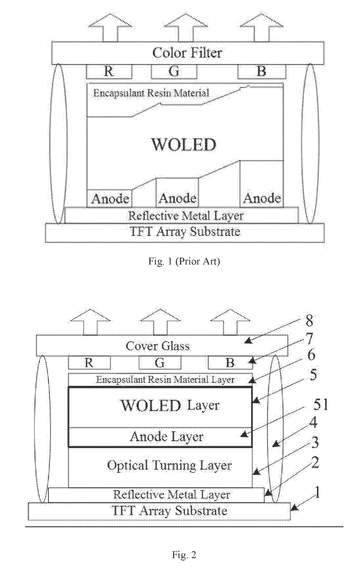
[0069]A WOLED layer 5 of the present embodiment comprises an anode layer 51, two light emitting units 52, one connection layer 54, and a cathode layer 53.
[0070]A light emitting unit 52 comprises a hole injection layer 525, a hole transport layer 524 formed on the hole injection layer 525, a light emitting layer 523 formed on the hole transport layer 524, an electron transport layer 522 formed on the light emitting layer 523, and an electron injection layer 521 formed on the electron transport layer 522.
[0071]The light emitting layer 523 is arranged between the electron transport layer 522 and the hole transport layer 524, and traditional host-guest doped dyes are thus placed.
[0072]The cathode layer 53 is formed on the electron injection layer 521 of a first light emitting unit 521. The first light emitting unit and a second light emitting unit are connected to each other by the connection layer. A hole injection layer 525 of the second light emitting unit is formed o...
embodiment 2
of WOLED Layer 5
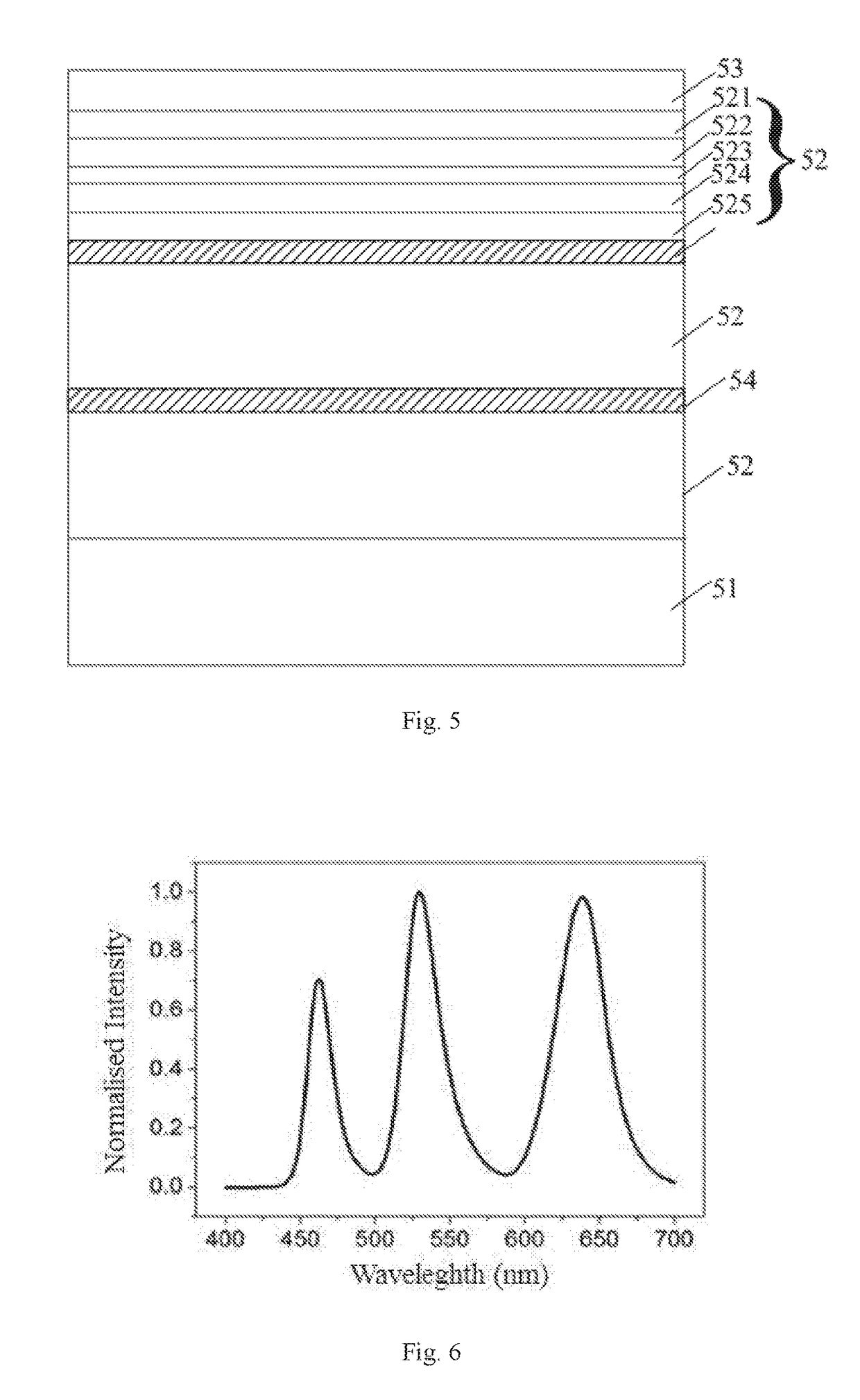
[0075]A WOLED layer 5 of the present embodiment comprises an anode layer 51, three light emitting units 52, two connection layers 54, and a cathode layer 53. A structure of a light emitting unit 52 is the same as that of Embodiment 1. A first light emitting unit and a second light emitting unit are connected to each other by a first connection layer, and the second light emitting unit and a third light emitting unit are connected to each other by a second connection layer, as shown in FIG. 5.
[0076]In the present embodiment, a light emitting layer of the first light emitting unit is made of a fluorescent material that emits red light; a light emitting layer of the second light emitting unit is made of a fluorescent material that emits green light; and a light emitting layer of the third light emitting unit is made of a fluorescent material that emits blue light. After mixing of the red light emitted by the first light emitting unit, the green light emitted by the seco...
PUM
 Abstract
Description
Claims
Application Information