Multiple (multi-) level cell (MLC) non-volatile (NV) memory (NVM) matrix circuits for performing matrix computations with multi-bit input vectors

a multi-level cell, matrix circuit technology, applied in the field of computerization of biological networks, can solve the problems of reducing affecting the scalability of the system, and unable to integrate thousands of dedicated synapse circuits per neuron, so as to avoid creating sneak path currents

Active Publication Date: 2019-01-17
QUALCOMM INC
View PDF2 Cites 69 Cited by
  • Summary
  • Abstract
  • Description
  • Claims
  • Application Information

AI Technical Summary

Benefits of technology

[0017]To multiply the multi-bit input vector of 1×n size times the m×n MLC NVM matrix circuit formed by the plurality of NVM storage string circuits, a line voltage is applied to the bit lines of the NVM storage string circuits while input voltages representing the input vector are applied to n×m word lines to be applied to respective gate nodes of the NVM bit cell circuits in respective MLC NVM storage circuits. This causes a summation current to be generated on each source line based on the weighted summed contribution of each MLC NVM storage circuit total resistance (based on the individual resistance of their respective NVM bit cell circuits) to its respective source line. Each output node forms an output vector, which is the result of the 1×n multi-bit input vector times one (1) column n of the m×n MLC NVM matrix circuit. By the NVM bit cell circuits of the MLC NVM storage circuits including a transistor coupled to a word line that controls the resistance contributed by its respective NVM storage string circuit on its respective source line, a cross-bar connection between the word lines and the bit lines does not have to be provided, which avoids creating sneak path currents in the MLC NVM matrix circuit. The word lines and the bit lines are isolated from each other through the NVM bit cell circuits of their respective MLC NVM storage circuits.

Problems solved by technology

Reproducing these biological features in neuromorphic electronic circuits presents a scaling problem, as integrating thousands of dedicated synapse circuits per neuron can quickly become infeasible for circuit systems that require a large number of neurons.
In conventional complementary metal oxide semiconductor (CMOS) circuit technology, this can lead to restrictions on scalability.
For example, microchip CMOS circuit implementations of STDP rules may result in about thirty (30) transistors per plastic synapse, and thus may lead to high costs for their hardware realization.
There is, overall, general thinking that STDP is very expensive to implement in conventional CMOS microchips.
It may not be possible to distinguish the sneak-current leading to an incorrect updating of the weight of the memristor cross-bar matrix circuit 212.
Further, RRAM technologies, such as memristors, may not have highly repeatable resistances leading to retention issues that can cause incorrect calculations.
Endurance of RRAM technologies may also be limited.

Method used


Image

  • Multiple (multi-) level cell (MLC) non-volatile (NV) memory (NVM) matrix circuits for performing matrix computations with multi-bit input vectors
  • Multiple (multi-) level cell (MLC) non-volatile (NV) memory (NVM) matrix circuits for performing matrix computations with multi-bit input vectors
  • Multiple (multi-) level cell (MLC) non-volatile (NV) memory (NVM) matrix circuits for performing matrix computations with multi-bit input vectors

Examples


Embodiment Construction

[0058]With reference now to the drawing figures, several exemplary aspects of the present disclosure are described. The word “exemplary” is used herein to mean “serving as an example, instance, or illustration.” Any aspect described herein as “exemplary” is not necessarily to be construed as preferred or advantageous over other aspects.

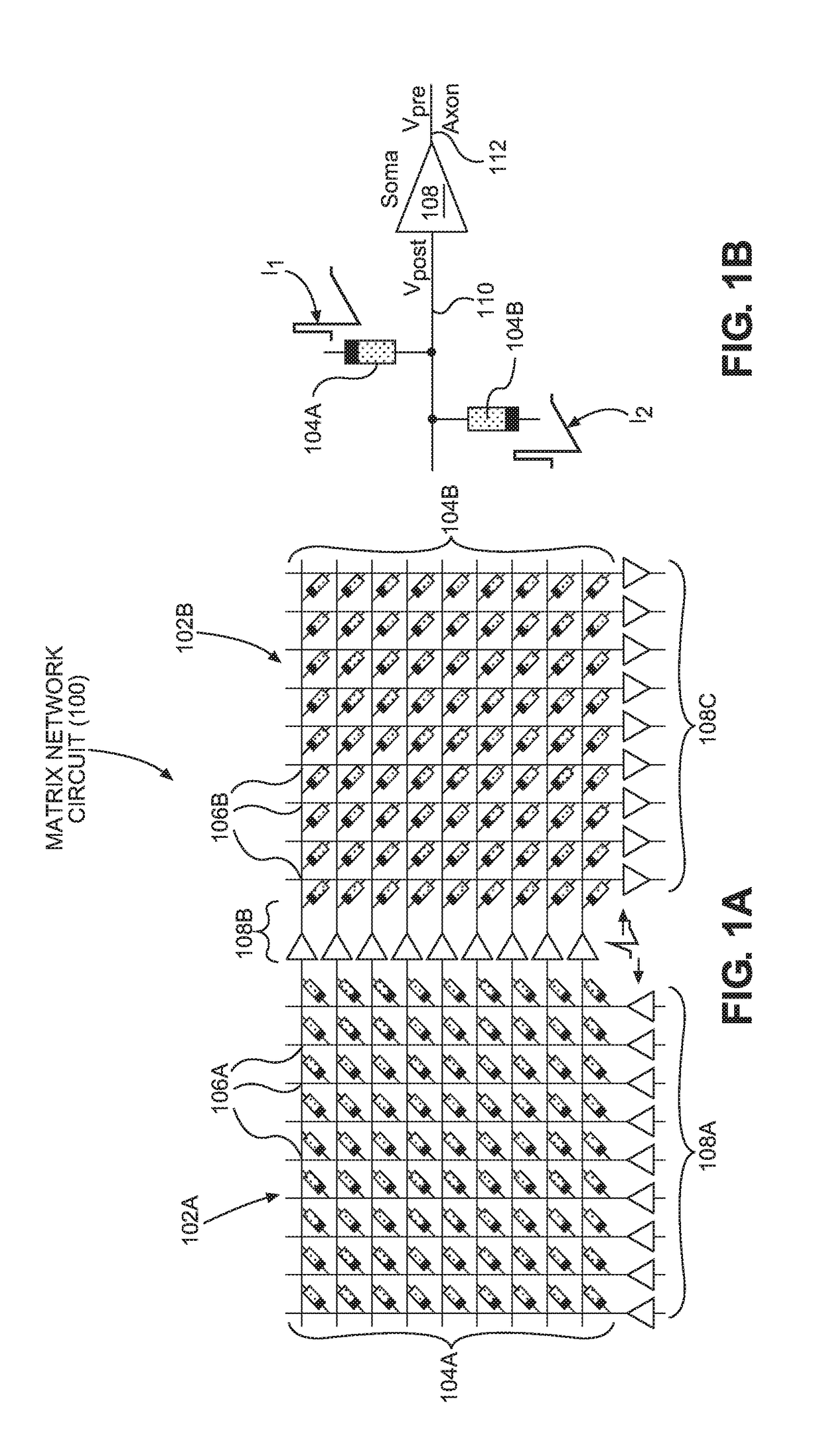
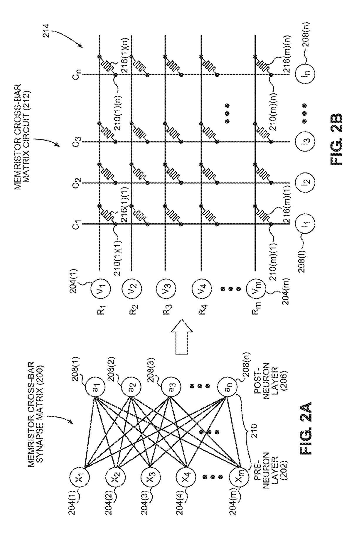
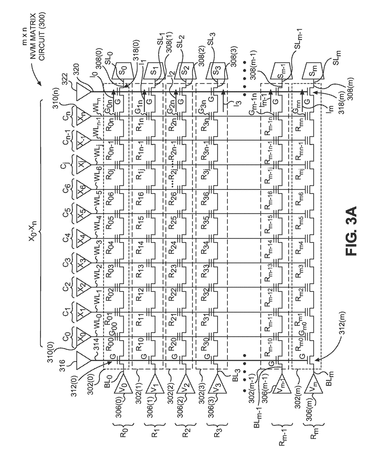
[0059]Aspects disclosed in the detailed description include multiple (multi-) level cell (MLC) non-volatile (NV) memory (NVM) matrix circuits for performing matrix computations with multi-bit input vectors. In exemplary aspects disclosed herein, an MLC NVM matrix circuit is provided that includes a plurality of NVM storage string circuits organized in respective memory rows. Each NVM storage string circuit includes a plurality of MLC NVM storage circuits. Thus, the plurality of MLC NVM storage circuits, which are each associated with an NVM storage string circuit, are arranged and addressable in respective memory rows and columns in the MLC NVM matrix...


PUM


Abstract

Multiple (multi-) level cell (MLC) non-volatile (NV) memory (NVM) matrix circuits for performing matrix computations with multi-bit input vectors are disclosed. An MLC NVM matrix circuit includes a plurality of NVM storage string circuits that each include a plurality of MLC NVM storage circuits each containing a plurality of NVM bit cell circuits each configured to store 1-bit memory state. Thus, each MLC NVM storage circuit stores a multi-bit memory state according to memory states of its respective NVM bit cell circuits. Each NVM bit cell circuit includes a transistor whose gate node is coupled to a word line among a plurality of word lines configured to receive an input vector. Activation of the gate node of a given NVM bit cell circuit in an MLC NVM storage circuit controls whether its resistance is contributed to total resistance of an MLC NVM storage circuit coupled to a respective source line.

Description

PRIORITY APPLICATION[0001]The present application claims priority under 35 U.S.C. § 119(e) to U.S. Provisional Patent Application Ser. No. 62 / 531,924 entitled “MULTI-LEVEL CELL (MLC) MATRIX MEMORY CIRCUITS EMPLOYING NON-VOLATILE (NV) MLC MEMORY CIRCUITS FOR PERFORMING MATRIX COMPUTATIONS” and filed on Jul. 13, 2017, which is incorporated herein by reference in its entirety.RELATED APPLICATIONS[0002]The present application is related to U.S. Provisional Patent Application Ser. No. 62 / 531,921 entitled “MATRIX MEMORY CIRCUITS EMPLOYING NON-VOLATILE (NV) MEMORY CIRCUITS FOR PERFORMING MATRIX COMPUTATIONS” and filed on Jul. 13, 2017, which is incorporated herein by reference in its entirety.[0003]The present application is also related to U.S. patent application Ser. No. 15 / 817,441 entitled “NON-VOLATILE (NV) MEMORY (NVM) MATRIX CIRCUITS EMPLOYING NVM MATRIX CIRCUITS FOR PERFORMING MATRIX COMPUTATIONS” and filed on Nov. 20, 2017, which is incorporated herein by reference in its entirety....

Claims


Application Information

Patent Timeline
Patent Type & Authority Applications(United States)
IPC IPC(8): G11C16/34G11C14/00G11C11/56G11C16/04H01L27/108H01L29/792H01L45/00
CPCG11C16/3481G11C14/0063G11C11/5628G11C16/0483H01L45/122H01L27/10826H01L29/7923H01L45/085G11C16/3459G06N3/063G11C5/02G11C5/063G11C7/1006G11C7/18G11C8/14G11C11/54H03K19/17736G06N3/049G06N3/084G11C16/0466G11C11/223G11C11/1653G11C13/0023G11C2213/79H10B12/36H10N70/245H10N70/821
Inventor LI, XIAKANG, SEUNG HYUKCHEN, WEI-CHUAN
Owner QUALCOMM INC
Why Eureka
Try Eureka