Bonded body and elastic wave element

a technology of elastic wave element and bonding body, which is applied in piezoelectric/electrostrictive/magnetostrictive devices, piezoelectric/electrostrictive/magnetostrictive devices, semiconductor devices, etc., can solve the problems of insufficient bonding strength and crack generation, and achieve the effect of improving the bonding strength of piezoelectric single crystal substrate and bonding layer, preventing separation, and improving the bonding strength

Active Publication Date: 2019-01-31
NGK INSULATORS LTD
View PDF0 Cites 10 Cited by
  • Summary
  • Abstract
  • Description
  • Claims
  • Application Information

AI Technical Summary

Benefits of technology

[0023]According to the present invention, in bonding a piezoelectric single crystal substrate and a supporting body made of a ceramic, it is provided a bonding layer composed of a material selected from the group consisting of mullite, alumina, tantalum pentoxide, titanium oxide and niobium pentoxide. It is thereby possible to improve a bonding strength of the piezoelectric single crystal substrate and bonding layer. At the same time, an arithmetic average roughness Ra of a surface of the supporting body is made 0.5 nm or larger and 5.0 nm or smaller, so that it is possible to prevent the separation at an interface of the supporting body and the specific bonding layer. Although the surface of the supporting body having Ra exceeding 5.0 nm is still said to be extremely smooth, it could have been still difficult to predict that the probability of the separation at the interface of the supporting body and specific bonding layer is considerably increased.

Problems solved by technology

However, in the case that the piezoelectric single crystal substrate is directly bonded to a supporting by made of a ceramic, cracks may be generated due to a difference of thermal expansion of the piezoelectric single crystal substrate and ceramic during heating after the bonding.
However, as the inventors actually tried to fabricate a bonded body, the bonding strength was proved to be still insufficient so that the separation occurred along an interface between the piezoelectric single crystal substrate and bonding layer during the subsequent processing steps.

Method used


Image

  • Bonded body and elastic wave element
  • Bonded body and elastic wave element
  • Bonded body and elastic wave element

Examples


example a1

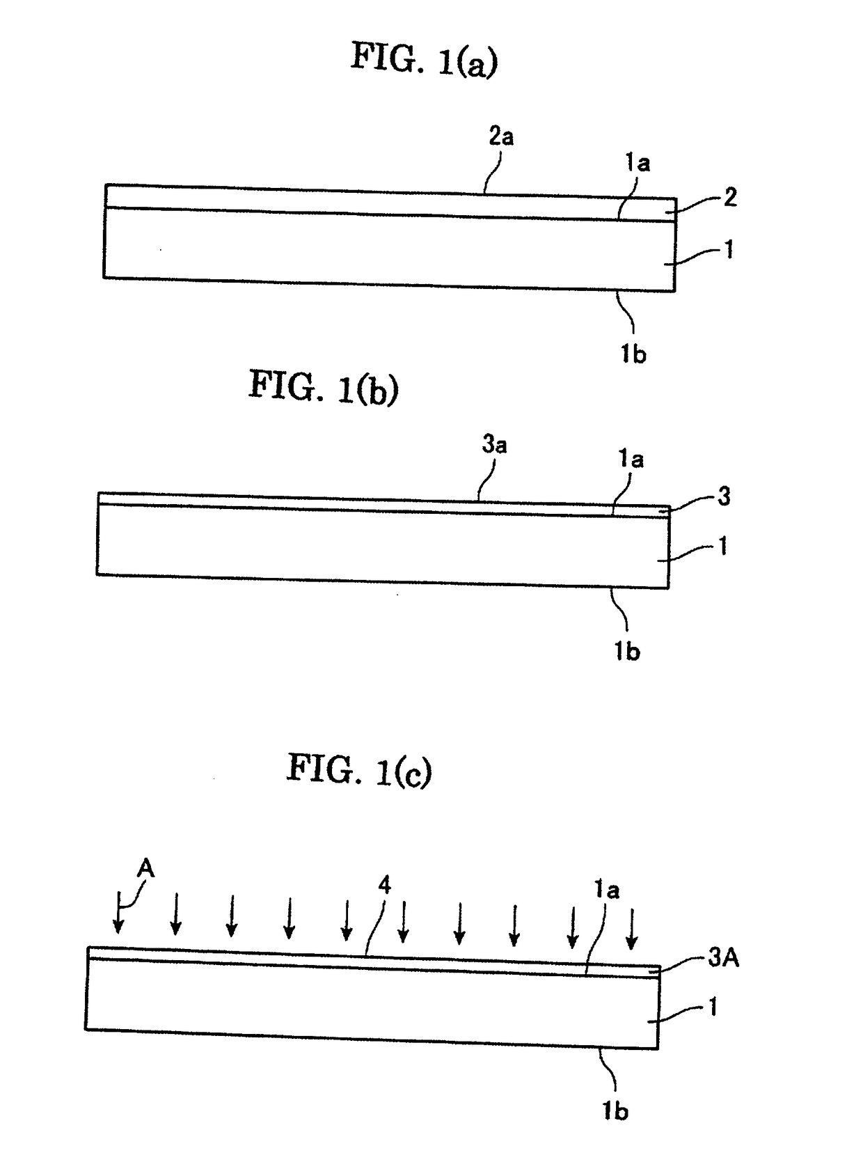
[0066]A bonded body was produced, according to the method described referring to FIGS. 1 and 2.

[0067]Specifically, a substrate (LT substrate) of lithium tantalate having an orientation flat (OF) part, a diameter of 4 inches and thickness of 250 μm was used as the piezoelectric single crystal substrate 6. As the LT substrate, it was used LT substrate of 46° Y-cut X-propagation LT substrate, in which the direction of propagation of the surface acoustic wave (SAW) is X and the Y-cut plate is rotated in a cutting angle. The surface 6a of the piezoelectric single crystal substrate 6 was mirror-polished to an arithmetic average roughness Ra of 0.3 nm.

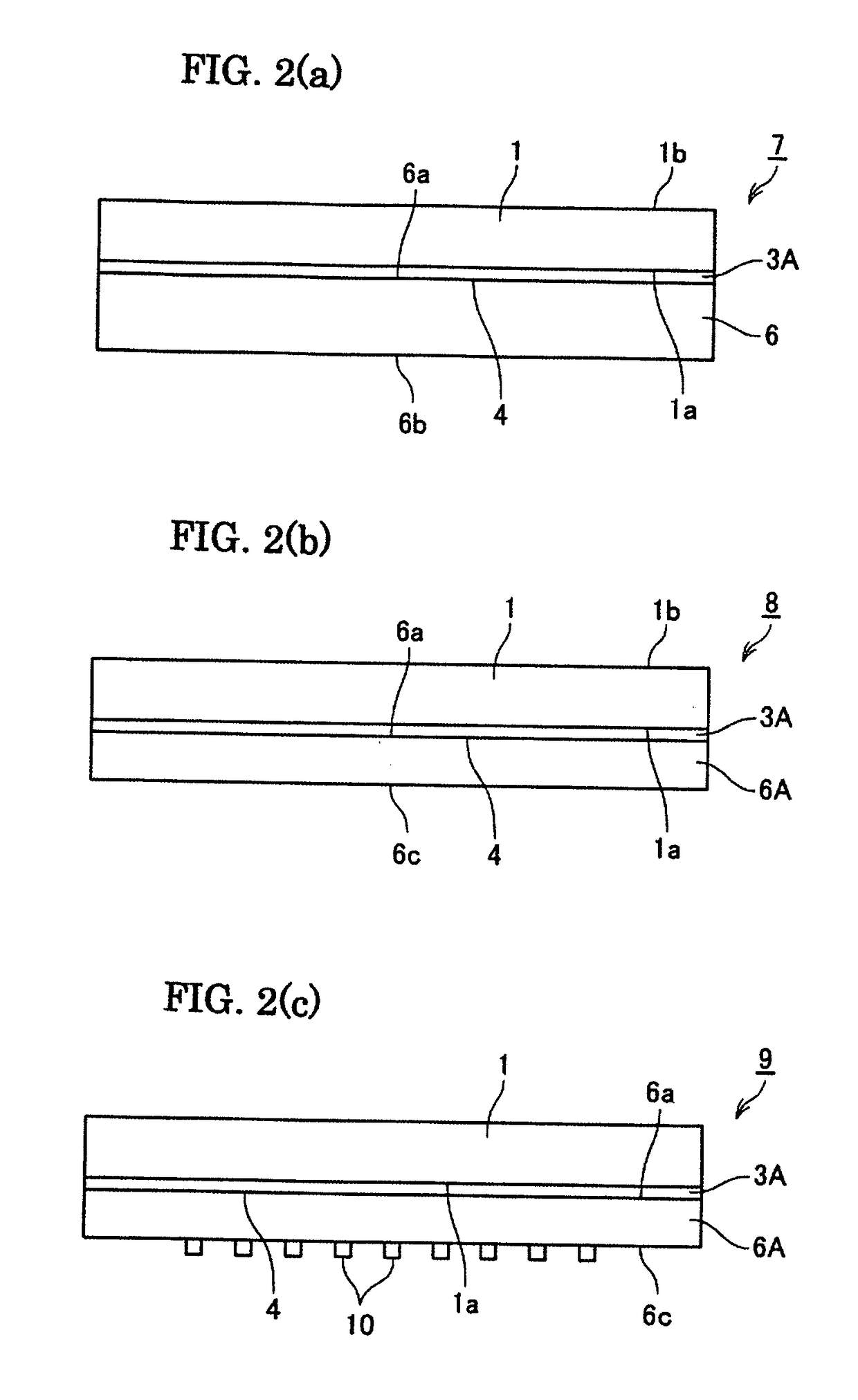
[0068]Further, as the supporting body 1, it was prepared a body 1 having an OF part, a diameter of 4 inches, a thickness of 230 μm and made of mullite. The arithmetic average roughness Ra and PV value of the surface 1a of the supporting body 1 of mullite were 0.5 nm and 10 nm, respectively. The arithmetic average roughness was measured by an ...

example a2

to A4 and Comparative Examples A1 to A4

[0074]In the Example A1, abrasives used for processing the surface of the supporting body was changed, so that Ra and PV value of the surface of the supporting body was changed as shown in table 1. The bonded bodies of the Examples A2 to A4 and Comparative Examples A1 to A4 were thus obtained. However, in the Comparative Example A4, the thickness of the bonding layer was changed to 300 μm.

[0075]The measurement of the bonding strength and tape peeling test were performed for the thus obtained bonded bodies. The results were shown in Table 1.

TABLE 1Ra ofPV value ofThick-surface ofsurface ofness ofsupportingsupportingbondingBondingbodybodylayerStrengthTape(nm)(nm)(nm)(J / m2)testExample A10.5101001.4NoseparationExample A20.8201001.8NoseparationExample A33.0301002.0NoseparationExample A45.0501001.4NoseparationCom. Ex. A10.3551001.4SeparatedCom. Ex. A27.0701000.7SeparatedCom. Ex. A312.01401000.2SeparatedCom. Ex. A412.01403001.4Separated

example b

[0076]In the Examples A1 to A4 and Comparative Examples A1 to A3, the material of the bonding layer 2 was made alumina, and the film-formation of the bonding layer 2 was performed by sputtering method. The other procedures were same as those in the Example A1 to produce the respective bonded bodies.

[0077]As a result, the separation of the bonded parts was not observed during the grinding and polishing steps of the piezoelectric single crystal substrate. Further, the results of the bonding strength by crack opening method and tape peeling test were comparable with those of the Examples A1 to A4 and Comparative Examples A1 to A3.


PUM

PropertyMeasurementUnit
arithmetic average roughness Raaaaaaaaaaa

Abstract

A bonded body includes a supporting body composed of a ceramic, a bonding layer provided over a surface of the supporting body and composed of one or more material selected from the group consisting of mullite, alumina, tantalum pentoxide, titanium oxide and niobium pentoxide, and a piezoelectric single crystal substrate bonded with the bonding layer. The surface of the supporting body has an arithmetic average roughness Ra of 0.5 nm or larger and 5.0 nm or smaller.

Description

CROSS-REFERENCE TO RELATED APPLICATIONS[0001]This is a continuation of International Application No. PCT / JP2017 / 006476, filed Feb. 22, 2017, which claims priority of Japanese Patent Application No. 2016-061713, filed Mar. 25, 2016, the entire contents of which are incorporated herein by reference.TECHNICAL FIELD[0002]The present invention relates to a bonded body of a piezoelectric single crystal substrate and a supporting body composed of a ceramic, and an acoustic wave device utilizing the same.BACKGROUND ARTS[0003]It is known a surface acoustic wave device functioning as a filter device or oscillator used in mobile phones or the like and an acoustic wave device such as lamb wave device or film bulk acoustic resonator (FBAR) using a piezoelectric thin film. As such acoustic wave device, it is known a device produced by adhering a supporting body and a piezoelectric substrate propagating a surface acoustic wave and by providing interdigitated electrodes capable of oscillating the s...

Claims


Application Information

Patent Timeline
Patent Type & Authority Applications(United States)
IPC IPC(8): H03H9/02H01L41/09H01L41/187H01L41/313H01L41/337H03H3/08H03H9/25
CPCH03H9/02574H01L41/09H01L41/187H01L41/313H01L41/337H03H3/08H03H9/25H03H9/02559H03H9/02834H10N30/073H10N30/20H10N30/853H10N30/086H10N30/01H03H9/02622Y10T29/42H01L24/83H01L21/2007
Inventor TAI, TOMOYOSHIGOTO, MASASHIUNO, YUDAIKANEKO, SHINYA
Owner NGK INSULATORS LTD
Why Eureka
Try Eureka