Material for forming underlayer film for lithography, composition for forming underlayer film for lithography, underlayer film for lithography and production method thereof, pattern forming method, resin, and purification method

Active Publication Date: 2019-02-07
MITSUBISHI GAS CHEM CO INC
View PDF7 Cites 1 Cited by
  • Summary
  • Abstract
  • Description
  • Claims
  • Application Information

AI Technical Summary

Benefits of technology

The present invention relates to a material that can be used to create a film for lithography during semiconductor manufacturing. This material can be applied in a wet process and results in a photoresist underlayer film that is highly resistant to heat and etching. The technical effect of this invention is the ability to form a robust and reliable film that protects the photoresist during the manufacturing process.

Problems solved by technology

Then, in lithography using exposure to light, which is currently used as a general-purpose technique, the resolution is now approaching the intrinsic limitation associated with the wavelength of the light source.
However, as the resist pattern is made finer and finer, there arise a problem of resolution and a problem of collapse of the resist pattern after development, and therefore there is demanded for making a resist film thinner.
Meanwhile, if the resist film is merely made thinner, it is difficult to achieve the resist pattern having a film thickness sufficient for processing a substrate.

Method used


Image

  • Material for forming underlayer film for lithography, composition for forming underlayer film for lithography, underlayer film for lithography and production method thereof, pattern forming method, resin, and purification method
  • Material for forming underlayer film for lithography, composition for forming underlayer film for lithography, underlayer film for lithography and production method thereof, pattern forming method, resin, and purification method
  • Material for forming underlayer film for lithography, composition for forming underlayer film for lithography, underlayer film for lithography and production method thereof, pattern forming method, resin, and purification method

Examples


example 11

[0333]Then, the composition for forming an underlayer film for lithography in Example 1 was coated on a SiO2 substrate having a film thickness of 300 nm, and baked at 240° C. for 60 seconds and further at 400° C. for 120 seconds to thereby form an underlayer film having a film thickness of 85 nm. A resist solution for ArF was coated on the underlayer film, and baked at 130° C. for 60 seconds to thereby form a photoresist layer having a film thickness of 140 nm. Herein, as the resist solution for ArF, one prepared by blending 5 parts by mass of the compound of the following formula (5), 1 part by mass of triphenylsulfonium nonafluoromethanesulfonate, 2 parts by mass of tributylamine, and 92 parts by mass of PGMEA was used.

[0334]A compound of formula (5) was prepared as follows. That is, 4.15 g of 2-methyl-2-methacryloyloxyadamantane, 3.00 g of methacryloyloxy-γ-butyrolactone, 2.08 g of 3-hydroxy-1-adamantyl methacrylate and 0.38 g of azobisisobutyronitrile were dissolved in 80 mL of ...

example 12

[0340]The composition for forming an underlayer film for lithography used in Example 1 was coated on a SiO2 substrate having a thickness of 300 nm, and baked at 240° C. for 60 seconds and further at 400° C. for 120 seconds to thereby form an underlayer film having a thickness of 90 nm. A silicon-containing intermediate layer material was coated on the underlayer film, and baked at 200° C. for 60 seconds to thereby form an intermediate layer film having a thickness of 35 nm. Furthermore, the resist solution for ArF was coated on the intermediate layer film, and baked at 130° C. for 60 seconds to thereby form a photoresist layer having a thickness of 150 nm. Herein, as the silicon-containing intermediate layer material, a silicon atom-containing polymer obtained below was used.

[0341]In 200 g of tetrahydrofuran (THF) and 100 g of pure water were dissolved 16.6 g of 3-carboxypropyltrimethoxysilane, 7.9 g of phenyltrimethoxysilane and 14.4 g of 3-hydroxypropyltrimethoxysilane, the liquid...


PUM

PropertyMeasurementUnit
Areaaaaaaaaaaa
Charge densityaaaaaaaaaa

Abstract

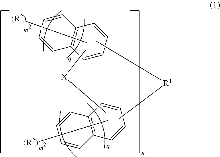
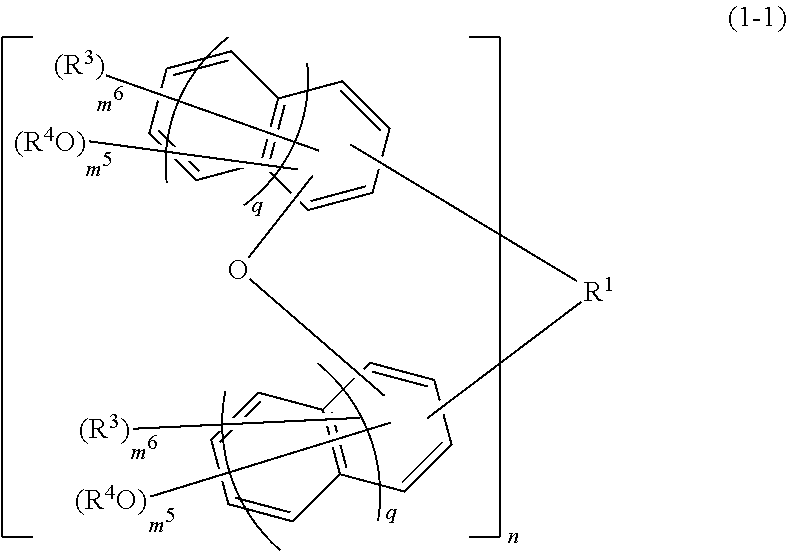
The present embodiment provides a material for forming an underlayer film for lithography, containing at least any of a compound represented by following formula (1) or a resin including a structural unit derived from a compound represented by the following formula (1),wherein R1 represents a 2n-valent group having 1 to 60 carbon atoms, or a single bond, each R2 independently represents a halogen atom, a straight, branched or cyclic alkyl group having 1 to 10 carbon atoms, an aryl group having 6 to 10 carbon atoms, an alkenyl group having 2 to 10 carbon atoms, an alkoxy group having 1 to 30 carbon atoms, a thiol group, a hydroxyl group, or a group where a hydrogen atom of a hydroxyl group is substituted with an acid-dissociable group, and may be the same or different in the same naphthalene ring or benzene ring, in which at least one R2 represents a group where a hydrogen atom of a hydroxyl group is substituted with an acid-dissociable group, n is an integer of 1 to 4, and structural formulae of n structural units in square brackets [ ] may be the same or different when n is an integer of 2 or more, X represents an oxygen atom, a sulfur atom, or an uncrosslinked state, each m2 is independently an integer of 0 to 7, provided that at least one m2 is an integer of 1 to 7, and each q is independently 0 or 1.

Description

TECHNICAL FIELD[0001]The present embodiment relates to a material for forming an underlayer film for lithography, a composition for forming an underlayer film for lithography, an underlayer film for lithography and a production method thereof, a pattern forming method, a resin, and a purification method.BACKGROUND ART[0002]Semiconductor devices are manufactured through microfabrication by lithography using a photoresist material, but are required to be made finer by a pattern rule in accordance with the increase in integration degree and the increase in speed of LSI in recent years. Then, in lithography using exposure to light, which is currently used as a general-purpose technique, the resolution is now approaching the intrinsic limitation associated with the wavelength of the light source.[0003]A light source for lithography, for use in forming a resist pattern, has a shorter wavelength from a KrF excimer laser (248 nm) to an ArF excimer laser (193 nm). However, as the resist patt...

Claims


Application Information

Patent Timeline
IPC IPC(8): G03F7/11C09D165/00C08G61/12C07D311/78C07D405/04G03F7/16G03F7/20G03F7/38G03F7/32H01L21/027H01L21/311H01L21/3213H01L21/768
CPCC07D311/78C08G61/122G03F7/16G03F7/168G03F7/2037H01L21/0276G03F7/322G03F7/38H01L21/31116H01L21/31144H01L21/32135H01L21/32139H01L21/76816H01L21/76877C08G2261/11C08G2261/148C08G2261/228C08G2261/3242C08G2261/71G03F7/11C09D165/00C07D405/04G03F7/094H01L21/027C08G61/02G03F7/26C07C37/72C07C39/12C07C39/14C07C69/96C08G8/08C08G8/14C08G8/18C08G61/00G03F7/0392G03F7/30G03F7/36
Inventor TOIDA, TAKUMIMAKINOSHIMA, TAKASHISATO, TAKASHIECHIGO, MASATOSHI
Owner MITSUBISHI GAS CHEM CO INC
Why Eureka
Try Eureka