

Active optical device enabled by dielectric metamaterials
a dielectric metamaterial and active optical technology, applied in the field of semiconductor devices, can solve the problems of inefficient light emission, visible and near infrared frequency resonators of dielectric metamaterials, etc., and achieve the effect of tolerating relatively large amounts of lattice strain
- Summary
- Abstract
- Description
- Claims
- Application Information
AI Technical Summary
Benefits of technology
Problems solved by technology
Method used
Image

Examples
example 1
Fabrication of GaAs Two-Dimensional Arrays
[0077]We fabricated GaAs two-dimensional dielectric resonator arrays using a combination of high-aspect-ratio etching and selective wet oxidation of AlGaAs under-layers to form a low refractive index oxide, i.e. native (AlxGa1-x)2O3 having a refractive index of about 1.6. As described in Example 2, below, we also used the same fabrication processes to demonstrate three-dimensional GaAs dielectric resonator arrays.
[0078]Our selective wet oxidation technique was adapted from a technique previously reported for forming current-blocking layers in vertical-cavity surface-emitting lasers. The earlier technique was reported, e.g., in the paper by K. D. Choquette et al., cited above.
[0079]FIG. 12 shows the process flow for creating GaAs resonators starting from a wafer, grown by molecular beam epitaxy (MBE), that consisted of a semi-insulating GaAs substrate onto which a 300-nm layer of Al0.85Ga0.15As was deposited followed by a 300 nm layer of GaAs...
example 2
Fabrication of Multilayer Arrays
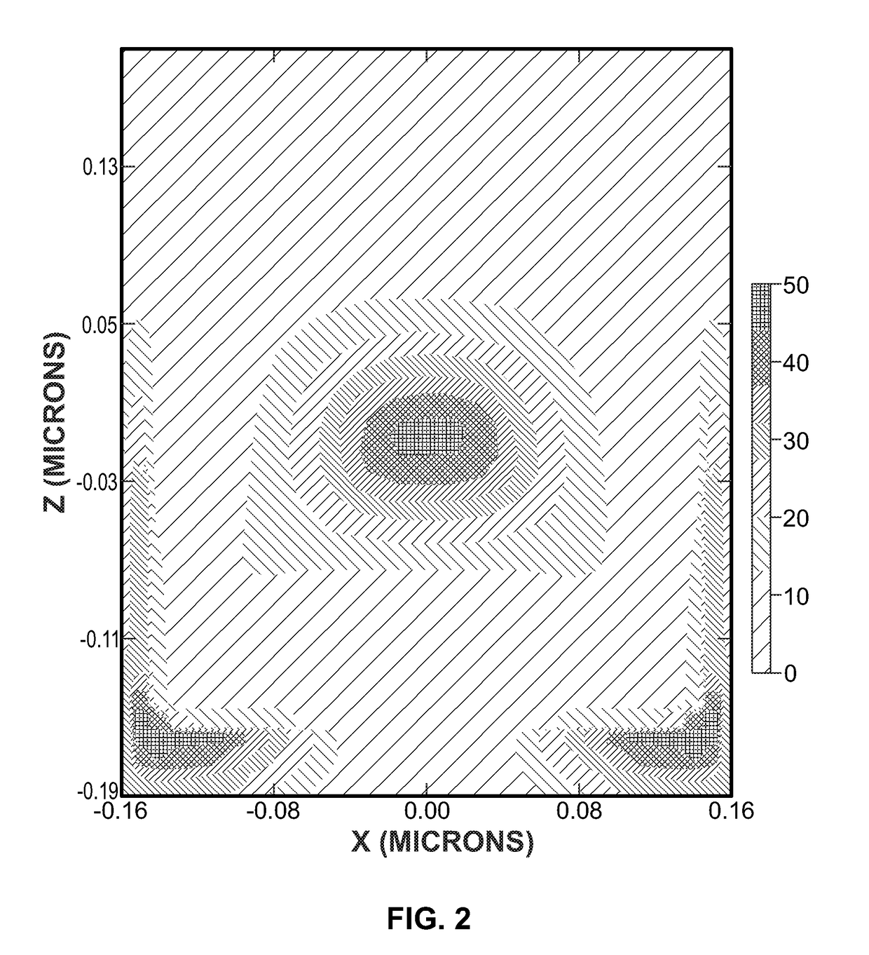
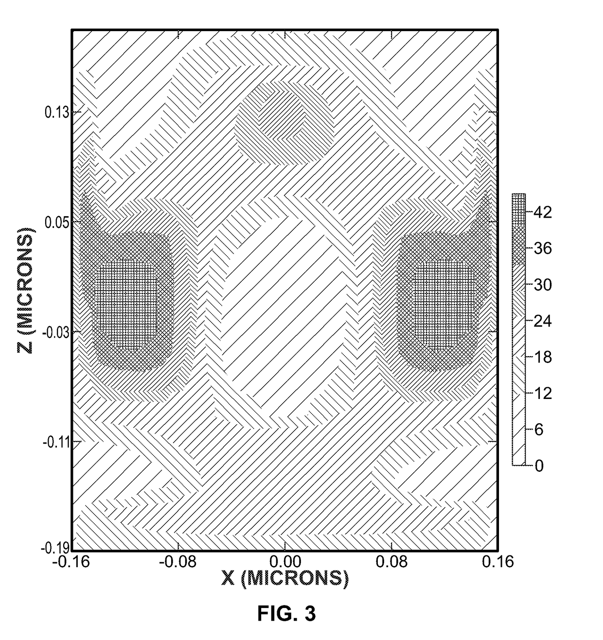
[0094]As mentioned above, fabricating three-dimensional dielectric metamaterials is possible using the techniques described here. By “three dimensional” structures we mean stacked multilayer structures (which are sometimes referred to as “quasi-three-dimensional”), as well as other kinds of structures that repeat in the direction perpendicular to the substrate.
[0095]To demonstrate the ability to produce multilayer dielectric resonator arrays, we fabricated monolithic arrays of columns on a GaAs substrate, in which each column contained three instances of the (AlxGa1-x)2O3—GaAs pattern described above in Example 1. That is, the sequence of layers in each column, from the bottom up, was GaAs / (AlxGa1-x)2O3 / GaAs / (AlxGa1-x)2O3 / GaAs / (AlxGa1-x)2O3 / GaAs. Our fabrication process was as described above in Example 1, except that the initial wafer had three layers of GaAs separated by three layers of AlGaAs.
[0096]FIG. 15 provides a view, based on a scanning elect...
example 3
Observation of Optical Transitions in Quantum Dots Multilayers in Cylindrical Resonators
[0100]FIG. 16 is a plot of six experimentally measured photoluminescent emission spectra of dielectric resonator arrays of the kind in which a gallium arsenide resonator layer includes a GaAs—InAs quantum dot multilayer. The dielectric resonators were cylindrical. Each spectrum corresponds to a respective cylinder diameter and pitch of the array.
[0101]The fluorescence was excited by optical pulses at about 850 nm.
[0102]Each of the spectra displays an emission peak at a respective wavelength determined by the resonator dimensions. As seen in the figure, a sharp emission peak occurs at the following wavelengths: for a cylinder diameter of 260 nm, about 1.120 μm; for a cylinder diameter of 280 nm, about 1.170 μm; for a cylinder diameter of 300 nm, about 1.250 μm; for a cylinder diameter of 320 nm, about 1.300 μm. When the cylinder diameter reaches 340 nm, a new resonance emerges, having a sharp emis...
PUM
 Abstract
Description
Claims
Application Information