Solid-state thin film hybrid electrochemical cell

a hybrid electrochemical cell and thin film technology, applied in the direction of electrochemical generators, electrochemical capacitors, electrical equipment, etc., can solve the problems that existing solid-state and semi-solid-state supercapacitors cannot meet all, wet supercapacitors cannot meet tough temperature requirements, and cannot be used for electric vehicles

Active Publication Date: 2019-02-14
THINIKA LLC
View PDF9 Cites 17 Cited by
  • Summary
  • Abstract
  • Description
  • Claims
  • Application Information

AI Technical Summary

Benefits of technology

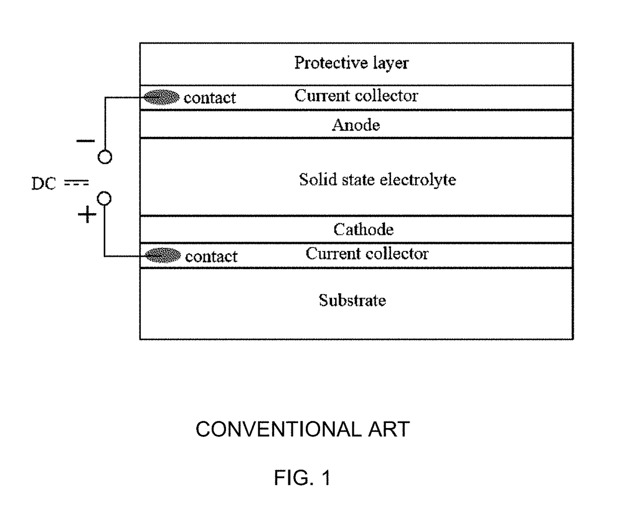
[0096]In a first broad aspect of the invention, there is provided an electrochemical power source comprising: a substrate; two current collector layers; two buffer / cache layers; a solid-state electrolyte layer, wherein each of the two buffer / cache layers is a layer of LiXMYO3, while M is selected among Nb, Ta, Ti, V; X is provided in the range of 0.8 to 1.4; and Y is provided in the range of 1.2 to 0.6, correspondingly.
[0097]In the ideal case, the buffer / cache layer material corresponds to formula LiXM(2-X)O3. However, it was proven experimentally that the invention is operable and the technical result is attained even if the ratio LiX:M(2-X) is not maintained for the Li0.8-1.4M1.2-0.6O3 material.
[0098]In such a power source, thickness of the buffer / cache layer may be in the range of 15 to 1000 nm, each layer may be in a form of a thin film, and the solid-state electrolyte layer may be an all-solid-state electrolyte layer.
[0099]Such a power source may further comprise at least one Faradaic layer, which may be a layer of WO2.4-2.9:M1:M2:E1:E2:E3, or MoO2.4-2.9:M1:M2:E1:E2:E3, wherein dopant M1 may be selected among Mo, Ti, Ni, V, Cr, Al, Nb, Ta, Co, Mn; dopant M2 may be selected among Mo, Ti, Ni, V, Cr, Al, Nb, Ta, Co, Mn; dopant E1 may be selected among H, N, C, Si, Ge, P, B; dopant E2 may be selected among H, N, C, Si, Ge, P, B; dopant E3 may be selected among H, N, C, Si, Ge, P, B, while M1 differs from M2 and E1, E2, E3 differ from each other. Thickness of the Faradaic layer may be in the range of 100 to 1000 nm.
[0100]The concentration of each of the dopants M1, M2 may be approx. 0.1% atomic to approx. 3% atomic, and preferably, their maximum concentration has to be evenly distributed over 30% or more of the Faradaic layer depth from the electrolyte side. Concentration of the dopants M1, M2 may be decreased (e.g., linearly or exponentially) at greater depth, but in the above-specified concentration range. Total content of dopants E1, E2, E3 may be approx. 3% atomic to approx. 40% atomic. Distribution of E1, E2, E3 atoms varies depending on the stored charge. In a charged state, E1, E2, E3 atoms concentrate at a border between the anode and the buffer / cache layer and / or drift into the anode structure. In a discharged state, E1, E2, E3 atoms concentrate at a border between the cathode and the buffer / cache layer and / or drift into the cathode structure.
[0101]In such a power source, each of the buffer / cache layers may be disposed between the solid-state electrolyte layer and the current collector layer or between the solid-state electrolyte layer and the Faradaic layer. The power source may further comprise an outer protective layer.

Problems solved by technology

Contrary to usual wet supercapacitors, thin film supercapacitors cannot be used for electric vehicles, massive power storages, energy boosters and so on.
Unfortunately, existing solid-state and semi-solid-state supercapacitors cannot meet all the above-mentioned requirements, and even wet supercapacitors cannot meet tough temperature requirements.

Method used


Image

  • Solid-state thin film hybrid electrochemical cell
  • Solid-state thin film hybrid electrochemical cell
  • Solid-state thin film hybrid electrochemical cell

Examples


example 1

[0219]An AS-TF-SS-PSC sample having structure as shown in FIG. 8A with dimensions of 30×30 mm was built on a Si / SiO2 substrate using a sputtered 250 nm titanium layer as a bottom and top current collectors. The sample was manufactured using the above-indicated technology; two buffer / cache layers having thickness of 20 nm were made of Li0.8Ta1.2O3. Faradic layer WO2.4:Al:N:C (500 nm) was sputtered from three targets, W, Al and Graphite, in Ar / O2 / N2 atmosphere by PDC reactive magnetron co-sputtering. Solid state electrolyte layer (400 nm) was RF sputtered from a Li3PO4 target in pure N2 atmosphere at +150° C. The sputtered sample was annealed at 200-250° C. in nitrogen atmosphere. The final device was laminated by the same material as used for pouch Li-ion battery production to avoid contact with environment. Measurements were performed according to the above-described methods. The sample had OCV of 2.9 V and ESR of 26 Ohm for 9 cm2 sample and was operational in the temperature range ...

example 2

[0220]An AS-TF-SS-PSC sample having structure as shown in FIG. 8A with dimensions of 30×30 mm was built on a Si / SiO2 substrate using a sputtered 250 nm titanium layer as bottom and top current collectors. The sample was manufactured using the above-described technology; two buffer / cache layers having thickness of 20 nm were made of Li1.0Ta1.0O3. Faradic layer WO2.4:Al:N:C (500 nm) was sputtered from three targets, W, Al and Graphite, in Ar / O2 / N2 atmosphere by PDC reactive magnetron co-sputtering. Solid state electrolyte layer (400 nm) was RF sputtered from a Li3PO4 target in pure N2 atmosphere at +150° C. The sputtered sample was annealed at 200-250° C. in nitrogen atmosphere. The final device was laminated by the same material as for pouch Li-ion battery production to avoid contact with environment. Measurements were performed according to the above-described methods. The sample had OCV of 3.1 V and ESR of 21 Ohm for 9 cm2 sample and was operational in the temperature range of −50 ...

example 3

[0221]An AS-TF-SS-PSC sample having structure as shown in FIG. 8A with dimensions of 30×30 mm was built on a Si / SiO2 substrate using a sputtered 250 nm titanium layer as a bottom and top current collectors. The sample was manufactured using the above-described technology; two buffer / cache layers having thickness of 20 nm were made of Li1.4Ta1.0O3. Faradic layer WO2.4:Al:N:C (500 nm) was sputtered from three targets, W, Al and Graphite, in Ar / O2 / N2 atmosphere by PDC reactive magnetron co-sputtering. Solid state electrolyte layer (400 nm) was RF sputtered from a Li3PO4 target in pure N2 atmosphere at +150° C. The sputtered sample was annealed at 200-250° C. in nitrogen atmosphere. The final device was laminated by the same material as that used for pouch Li-ion battery production to avoid contact with environment. Measurements were performed according to the above-described methods. The sample had OCV of 3.3 V and ESR of 18 Ohm for 9 cm2 sample and was operational in the temperature r...


PUM


Abstract

Thin film all-solid-state power sources, including pseudocapacitors having solid inorganic Li+-ion conductive electrolyte, for IoT, microsensors, MEMS, RFID TAGs, medical devices, elements of microfluidic chips Micro Electro Harvesting and ultra-light energy storage. An electrochemical power source includes a substrate; a first current collector layer on the substrate; a first buffer / cache layer on the first current collector layer; a solid-state electrolyte layer on the first buffer / cache layer; a second buffer / cache layer on the solid-state electrolyte layer; a second current collector layer on the second buffer / cache layer. Each buffer / cache layer is formed of LiXMYO3, where M is Nb, Ta, Ti, V, X is 0.8-1.4, and Y is 1.2-0.6. The buffer / cache layer is 15-1000 nm. At least one Faradaic layer is between the first collector layer and the first buffer layer and / or between the second collector layer and the second buffer layer.

Description

CROSS-REFERENCE TO RELATED APPLICATIONS[0001]This application claims priority to U.S. Provisional Application No. 62 / 544,998, filed on Aug. 14, 2017, which is incorporated herein by reference in its entirety.BACKGROUND OF THE INVENTIONField of the Invention[0002]The invention relates to thin film all-solid-state power sources, and, in particular, to thin film pseudocapacitors having solid inorganic Li+-ion electrolyte, intended for microelectronic devices (including micro sensors, micro electromechanical systems, microfluidic chips, RFID tags), various micro-electric harvesting solutions and ultra-light energy storage devices, medical devices and integrated solutions, such as monochip and lab-on-chip solutions.Background of the Related Art[0003]Miniaturization of electronic devices and reducing their power consumption require emerging sub-compact power sources suitable for direct embedding into microelectronic devices. Li-ion batteries and supercapacitors (i.e., electric double-laye...

Claims


Application Information

Patent Timeline
Patent Type & Authority Applications(United States)
IPC IPC(8): H01M10/0562H01M10/0525H01M10/058H01M4/36H01M4/66H01G11/06H01G11/56H01G11/46H01G11/68H01G11/84
CPCH01M4/661H01M10/0562H01M10/0525H01M10/058H01G11/68H01G11/84H01G11/06H01G11/56H01G11/46H01M4/36H01M4/485H01M10/0585H01M6/40Y02E60/13Y02E60/10Y02P70/50
Inventor MESHCHERYAKOV, VLADIMIR IGOREVICHROSSOUW, ARNOUXMANAKHOV, ANTON MIKHAILOVICHPOGORELOV, NIKOLAY ANATOLIEVICHKOLESNIKOVA, ELENA VIKTOROVNACHUGUNOV, VLADIMIR ALEKSANDROVICH
Owner THINIKA LLC
Why Eureka
Try Eureka