

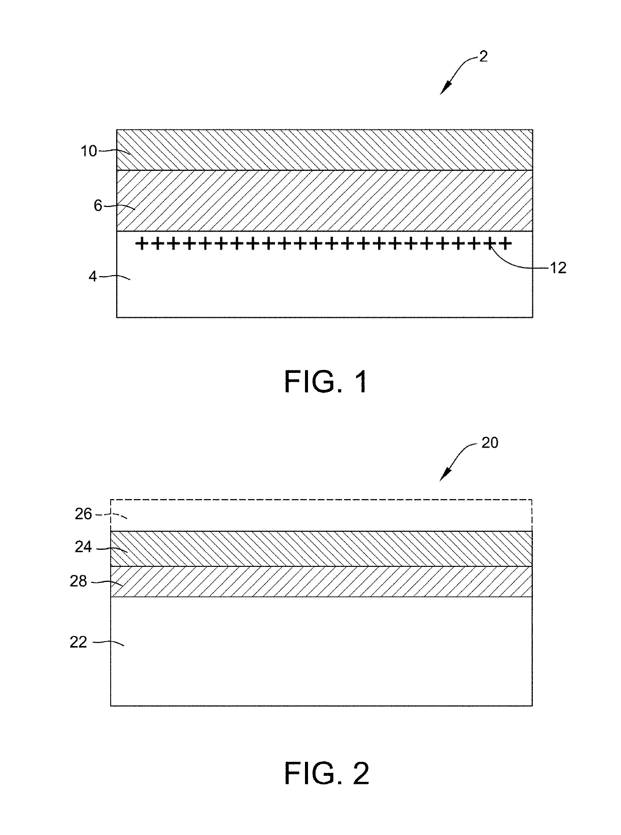
Method of depositing charge trapping polycrystalline silicon films on silicon substrates with controllable film stress
a polycrystalline silicon and film stress technology, applied in the field of semiconductor wafer manufacturing, can solve the problems of wasting one of the substrates, not having suitable thickness uniformity, and time-consuming and costly methods
- Summary
- Abstract
- Description
- Claims
- Application Information
AI Technical Summary
Benefits of technology
Problems solved by technology
Method used
Image

Examples
example 1
[0059]In one example, a silicon wafer sliced from an ingot grown by the Czochralski method is cleaned using SC1 solution. The cleaning is sufficient to obtain a chemical silicon oxide layer having a thickness between 0.8 nm and 2.0 nm on the front surface of the silicon wafer. The wafer is next loaded into a chemical vapor deposition chamber. The wafer is heated up to a temperature from 850° C. to 1000° C. Once the temperature set point is reached, the wafer is baked at the same temperature for between 5 seconds to 60 seconds, preferably between 10 seconds to 40 seconds. The ambient atmosphere in the CVD chamber is either H2 or a combination of H2 and an etching gas such as HCl or Cl2. The reducing atmosphere, which optionally comprises etching gas, is introduced to the chamber to removal wafer surface contamination. When the bake is complete, the wafer is subject to chemical vapor deposition of polycrystalline silicon at the same temperature as the reducing atmosphere bake. The sil...
example 2
[0060]In one example, a silicon wafer sliced from an ingot grown by the Czochralski method is cleaned using SC1 solution. The cleaning is sufficient to obtain a chemical silicon oxide layer having a thickness between 0.8 nm and 2.0 nm on the front surface of the silicon wafer. The wafer is next loaded into a chemical vapor deposition chamber. The wafer is heated up to a temperature from 850° C. to 1000° C. Once the temperature set point is reached, the wafer is baked at the same temperature for between 5 seconds to 60 seconds, preferably between 10 seconds to 40 seconds. The ambient atmosphere in the CVD chamber is either H2 or a combination of H2 and an etching gas such as HCl or Cl2. The reducing atmosphere, which optionally comprises etching gas, is introduced to the chamber to removal wafer surface contamination. When the bake is complete, the wafer is subject to chemical vapor deposition of polycrystalline silicon at the same temperature as the reducing atmosphere bake. The sil...
example 3
[0061]In one example, a silicon wafer sliced from an ingot grown by the Czochralski method is cleaned using SC1 solution. The cleaning is sufficient to obtain a chemical silicon oxide layer having a thickness between 0.8 nm and 2.0 nm on the front surface of the silicon wafer. The wafer is next loaded into a chemical vapor deposition chamber. The wafer is heated up to a temperature from 850° C. to 1000° C. Once the temperature set point is reached, the wafer is baked at the same temperature for between 5 seconds to 60 seconds, preferably between 10 seconds to 40 seconds. The ambient atmosphere in the CVD chamber is either H2 or a combination of H2 and an etching gas such as HCl or Cl2. The reducing atmosphere, which optionally comprises etching gas, is introduced to the chamber to removal wafer surface contamination. When the bake is complete, the wafer is subject to chemical vapor deposition of polycrystalline silicon seed at the same temperature as the reducing atmosphere bake. Th...
PUM
 Abstract
Description
Claims
Application Information