

Method For Producing Metal Nanoparticle-Polymer Composite Thin Film
- Summary
- Abstract
- Description
- Claims
- Application Information
AI Technical Summary
Benefits of technology
Problems solved by technology
Method used
Image

Examples
example 1
n of Gold Nanoparticle-Polymer Composite Thin Film
[0036](1) Production of Composite Thin Film in Reactor
[0037]Triton X-100 (Sigma-Aldrich, USA) was added to [BMIM]BF4 (1-butyl-3-methylimidazolium tetrafluoroborate, Sigma-Aldrich) to a final concentration of 6.0 mol %, followed by stirring using a vortex mixer (KMC-1300V) for 15 minutes. 10 mg of HAuCl4.xH2O (M.W.=339.79, Sigma-Aldrich) was added to 2.943 mL of the mixture solution, followed by sonication for 15 minutes.
[0038]0.5 ml of the prepared solution was placed in a Teflon reactor (70 mm×15 mm) and treated with plasma using an atmospheric-pressure plasma system (Ar, 150 W, 5 lpm) for 10 minutes. The distance between the plasma electrode and the liquid was 2 mm. After the plasma treatment, a film floating in the reactor was separated, washed sequentially with water and ethanol, and dried at 60° C. for 1 hour.
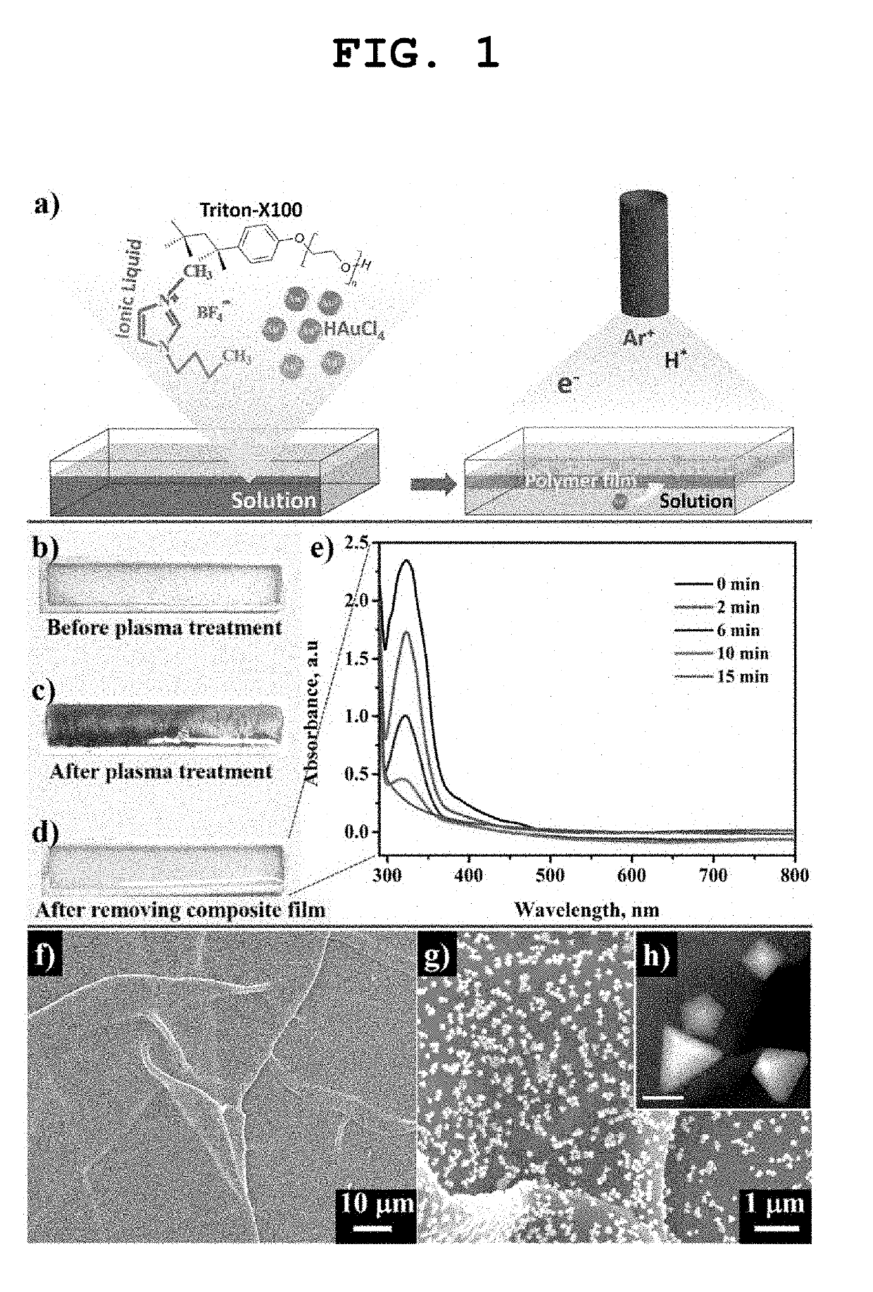
[0039]FIG. 1a) is a schematic view of the above-described reaction, and FIGS. 1b) and 1d) are photographs of an actual re...
example 2
l Analysis of Gold Nanoparticle-Polymer Composite Thin Film
[0044]The thin film produced in Example 1-(1) was imaged with low-magnification and high-magnification SEM (JSM-7000F, JEOL, Japan), and the images are shown in FIGS. 1f) and 1g). A TEM (JSM-7000F, JEOL, Japan) image of nanoparticles included in the thin film is shown in FIG. 1h). Wrinkles observed in FIG. if) were those formed in a process of transferring the thin film onto a silicon wafer for SEM image observation, and the SEM images of FIGS. 1f) and 1g) shows that particles having a uniform size were uniformly dispersed in the polymer thin film without being agglomerated. The scale bar in FIG. 1h) showing the TEM image indicates 100 nm, and suggests that Au nanoparticles had a particle size of about 100 nm and a clearly defined shape.
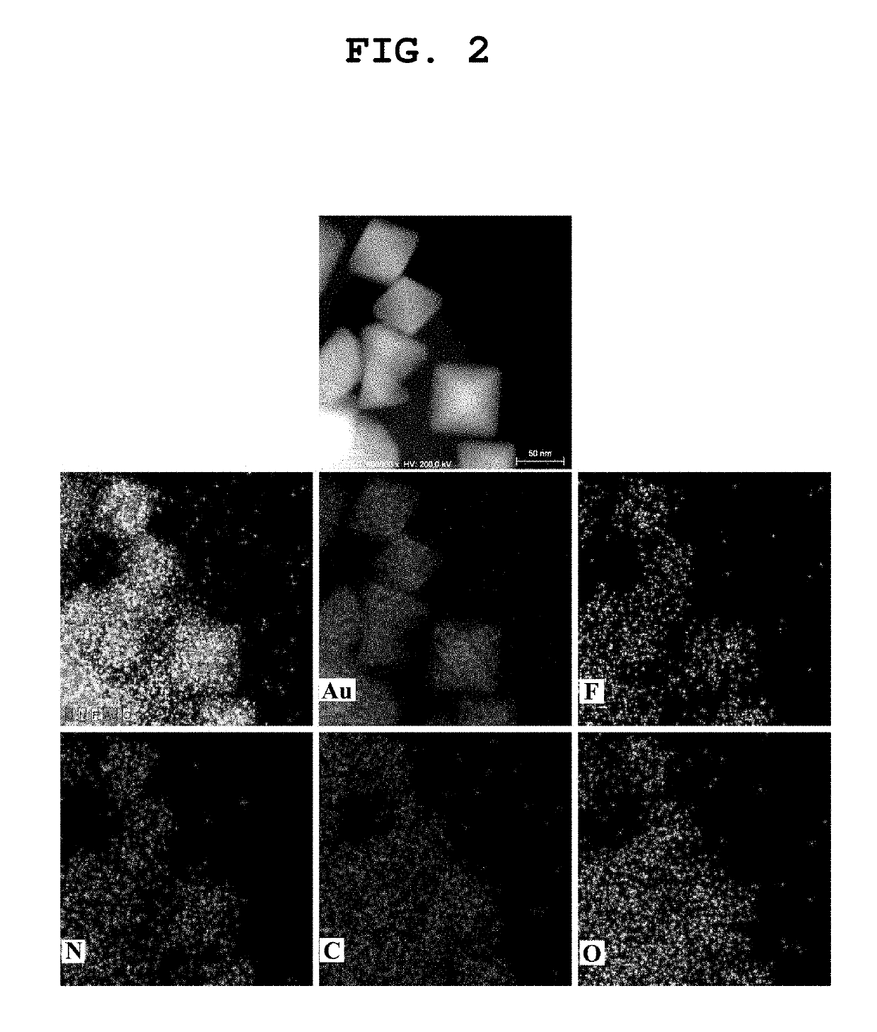
[0045]The components of the produced thin film were analyzed by STEM-EDS (scanning transmission electron microscopy energy dispersive spectrometry). FIG. 2 depicts STEM-EDS mapping images, an...
example 3
of Growth of Gold Nanoparticles for Varying Plasma Treatment Times
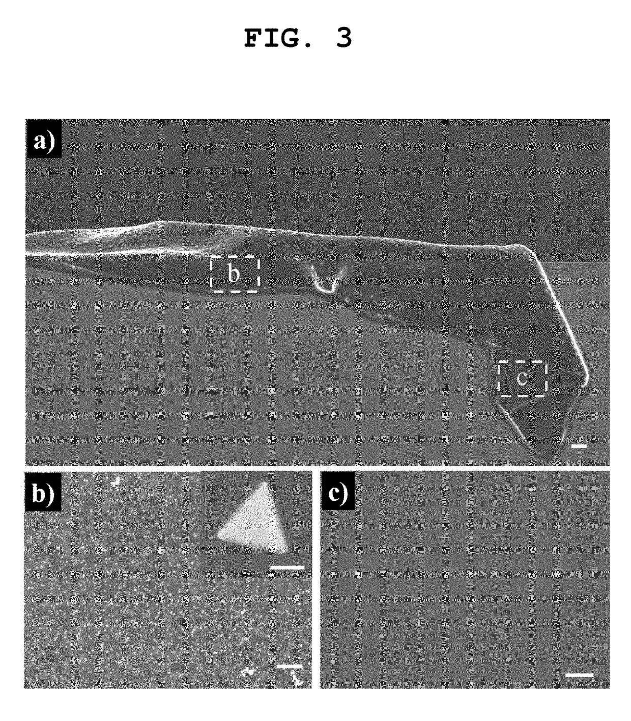
[0048]In order to examine the process of growth of gold nanoparticles in a polymer matrix, gold nanoparticle-polymer composite thin films were produced while changing the plasma treatment time to 2 min, 6 min, 10 min and 15 min. The produced gold nanoparticle-polymer composite thin films were observed with SEM and TEM, and the results of the observation are sequentially shown in FIGS. 5a) to 5d). The content of Triton X-100 relative to [BMIM]BF4 was 6 mol %, and the concentration of the gold nanoparticle precursor was 10 mM.
[0049]It was clearly observed that gold nanoparticles were formed after 2 minutes of plasma irradiation. It can be seen that the gold nanoparticles had an irregular shape and a size of about 20 nm and were single-twinned particles uniformly dispersed in the polymer thin film. When plasma was irradiated for 6 minutes, the size of the gold nanoparticles increased to about 60 nm, and the shape of the ...
PUM
 Abstract
Description
Claims
Application Information