Light irradiation type heat treatment method and heat treatment apparatus

a heat treatment method and heat treatment technology, applied in electrical apparatus, conveyor parts, testing/measurement of semiconductor/solid-state devices, etc., can solve problems such as cracking of semiconductor wafers, and high junction depths, and achieve quick grasping of the behavior of substrates. , the effect of simplifying the configuration

Active Publication Date: 2019-05-23
DAINIPPON SCREEN MTG CO LTD
View PDF11 Cites 8 Cited by
  • Summary
  • Abstract
  • Description
  • Claims
  • Application Information

AI Technical Summary

Benefits of technology

[0019]It is therefore an object of the present invention to quickly grasp the behavior of a substrate subjected to flash irradiation with a simplified configuration.

Problems solved by technology

This results in a junction depth much greater than a required depth, which might constitute a hindrance to good device formation.
There arises a problem such that cracking occurs in a semiconductor wafer when the semiconductor wafer vibrates severely or jumps up greatly from the susceptor to fall off.
Even if such wafer cracking does not result, there are cases in which the semiconductor wafer, once jumping up, falls onto the susceptor to be displaced (misaligned) from its original set position.
A large displacement of the semiconductor wafer from its original set position causes transport trouble, and might lead to not only breakage of the semiconductor wafer but also a hindrance to a transport robot in some cases.
However, such a high-speed camera is costly.
This not only leads to an increase in costs of the apparatus but also gives rise to a problem such that the analysis of captured image data is a complicated process.
Further, there is a need to obtain space for placement of the high-speed camera in the chamber.

Method used


Image

  • Light irradiation type heat treatment method and heat treatment apparatus
  • Light irradiation type heat treatment method and heat treatment apparatus
  • Light irradiation type heat treatment method and heat treatment apparatus

Examples


Embodiment Construction

[0032]A preferred embodiment according to the present invention will now be described in detail with reference to the drawings.

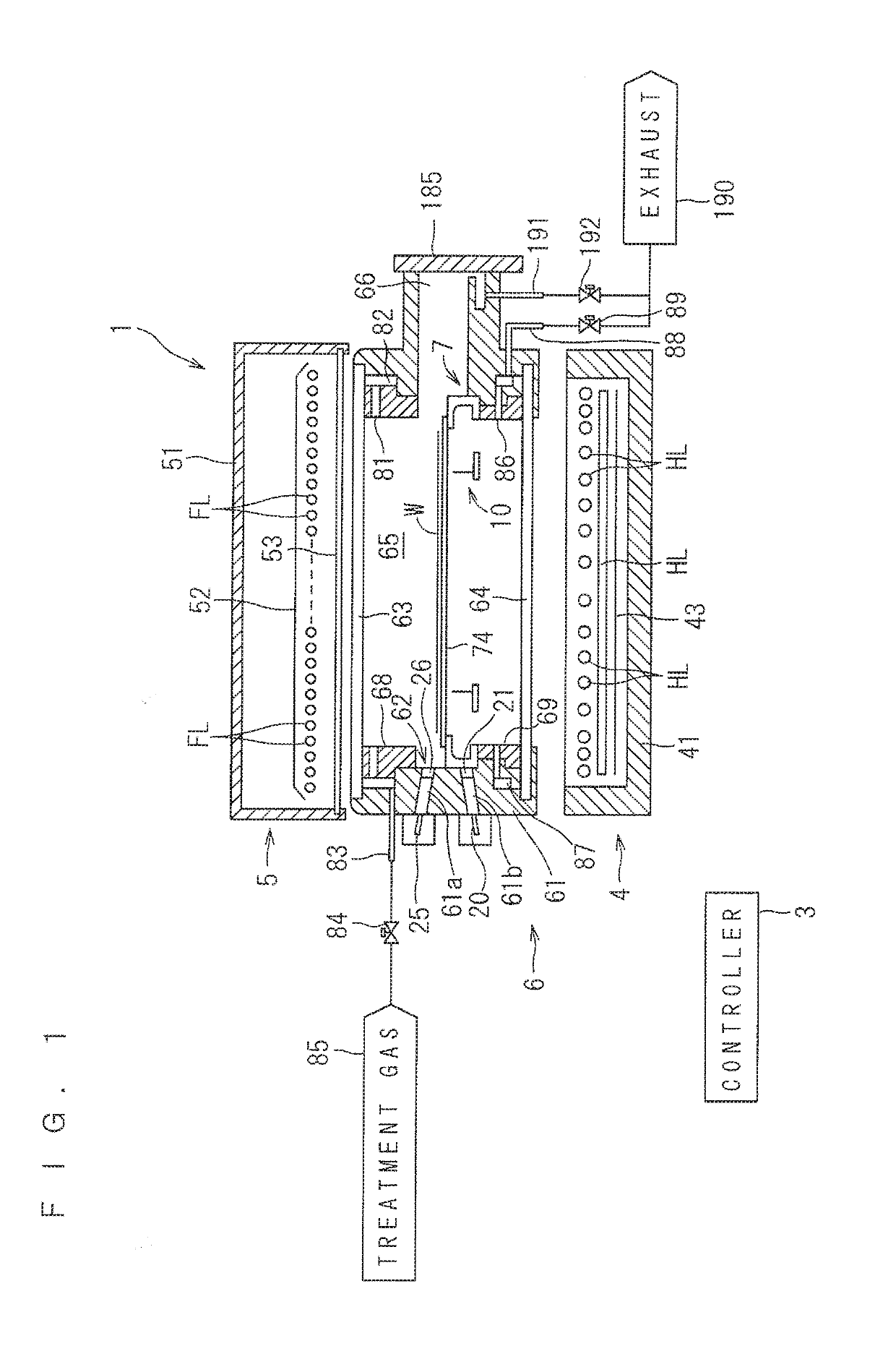
[0033]FIG. 1 is a longitudinal sectional view showing a configuration of a heat treatment apparatus 1 according to the present invention. The heat treatment apparatus 1 of FIG. 1 is a flash lamp annealer for irradiating a disk-shaped semiconductor wafer W serving as a substrate with flashes of light to heat the semiconductor wafer W. The size of the semiconductor wafer W to be treated is not particularly limited. For example, the semiconductor wafer W to be treated has a diameter of 300 mm and 450 mm (in the present preferred embodiment, 300 mm). The semiconductor wafer W prior to the transport into the heat treatment apparatus 1 is implanted with impurities. The heat treatment apparatus 1 performs a heating treatment on the semiconductor wafer W to thereby activate the impurities implanted in the semiconductor wafer W. It should be noted that the dimensions...


PUM


Abstract

A front surface of a semiconductor wafer is momentarily heated by irradiation with a flash of light from flash lamps. An upper radiation thermometer and a high-speed radiation thermometer unit measure a temperature of the front surface of the semiconductor wafer after the irradiation with the flash of light. The temperature data are sequentially accumulated, so that a temperature profile is acquired. An analyzer determines the highest measurement temperature of the semiconductor wafer subjected to the flash irradiation from the temperature profile to calculate a jump distance of the semiconductor wafer from a susceptor, based on the highest measurement temperature. If the calculated jump distance is greater than a predetermined threshold value, there is a high probability that the semiconductor wafer is significantly out of position, so that the transport of the semiconductor wafer to the outside is stopped.

Description

BACKGROUND OF THE INVENTIONField of the Invention[0001]The present invention relates to a heat treatment method and a heat treatment apparatus which irradiate a thin plate-like precision electronic substrate (hereinafter referred to simply as a “substrate”) such as a semiconductor wafer with a flash of light to heat the substrate.Description of the Background Art[0002]In the process of manufacturing a semiconductor device, impurity doping is an essential step for forming a pn junction in a semiconductor wafer. At present, it is common practice to perform impurity doping by an ion implantation process and a subsequent annealing process. The ion implantation process is a technique for causing ions of impurity elements such as boron (B), arsenic (As) and phosphorus (P) to collide against the semiconductor wafer with high acceleration voltage, thereby physically implanting the impurities into the semiconductor wafer. The implanted impurities are activated by the subsequent annealing pro...

Claims


Application Information

Patent Timeline
Patent Type & Authority Applications(United States)
IPC IPC(8): H01L21/66H01L21/324H01L21/67H01L21/677
CPCH01L22/12H01L21/324H01L21/67115H01L21/67248H01L21/67739H01L21/68785H01L21/6875H01L21/2686H01L21/67098
Inventor KAWARAZAKI, HIKARU
Owner DAINIPPON SCREEN MTG CO LTD
Why Eureka
Try Eureka