Fully-Printed Stretchable Thin-Film Transistors and Integrated Logic Circuits

a technology of intrinsically stretchable and fully printed thin films, applied in the direction of logic circuits characterised by logic functions, semiconductor devices, semiconductor/solid-state device details, etc., can solve the problems of large-area and low-cost fabrication of high-performance intrinsically stretchable electronic devices, no reliable high-performance and robust stretchable electronic material platform,

Active Publication Date: 2019-05-23
BOARD OF TRUSTEES OPERATING MICHIGAN STATE UNIV
View PDF0 Cites 3 Cited by
  • Summary
  • Abstract
  • Description
  • Claims
  • Application Information

AI Technical Summary

Benefits of technology

[0010]In accordance with an example, a thin-film device comprises: a stretchable polydimethylsiloxane (PDMS) substrate; and one or more thin-film transistor elements having a source, a drain, and/or a gate electrode formed of carbon nanotubes (CNTs) and having a stretchable hybrid gate dielectric, the one or more thin-film transistor elements being printed on the PDMS substrate and forming one or more stretchable thin-film transistor elements.
[0011]In accordance with another example, a thin-film device comprises: a stretchable elastomer substrate; and one or more thin-film transistor elements having a source, a drain, and/or a gate electrode formed of carbon nanotubes (CNTs) and having a stretchable hybrid gate dielectric, the one or more thin-film transistor elements being printed on the stretchable elastomer substrate and forming one or more stretchable thin-film transistor elements.
[0012]In accordance with another example, a method of formulating a printable stretchable dielectric layer ink, the method comprises: mixing barium titanate nanoparticles (BaTiO3) with polydimethylsiloxane (PDMS) and 4-methyl-2-pentanon...

Problems solved by technology

Nevertheless, the large-area and low-cost fabrication of high-performance intrinsically stretchable electronic devices has remained extremely difficult.
Researchers face a number of technical challenges when trying to develop large-area stretchable electronics.
There are no reliable high-performance and robust stretchable electronic material platforms.
And, there are no mechanisms to integrate standalone stretchable devices into functional sys...

Method used


Image

  • Fully-Printed Stretchable Thin-Film Transistors and Integrated Logic Circuits
  • Fully-Printed Stretchable Thin-Film Transistors and Integrated Logic Circuits
  • Fully-Printed Stretchable Thin-Film Transistors and Integrated Logic Circuits

Examples


Embodiment Construction

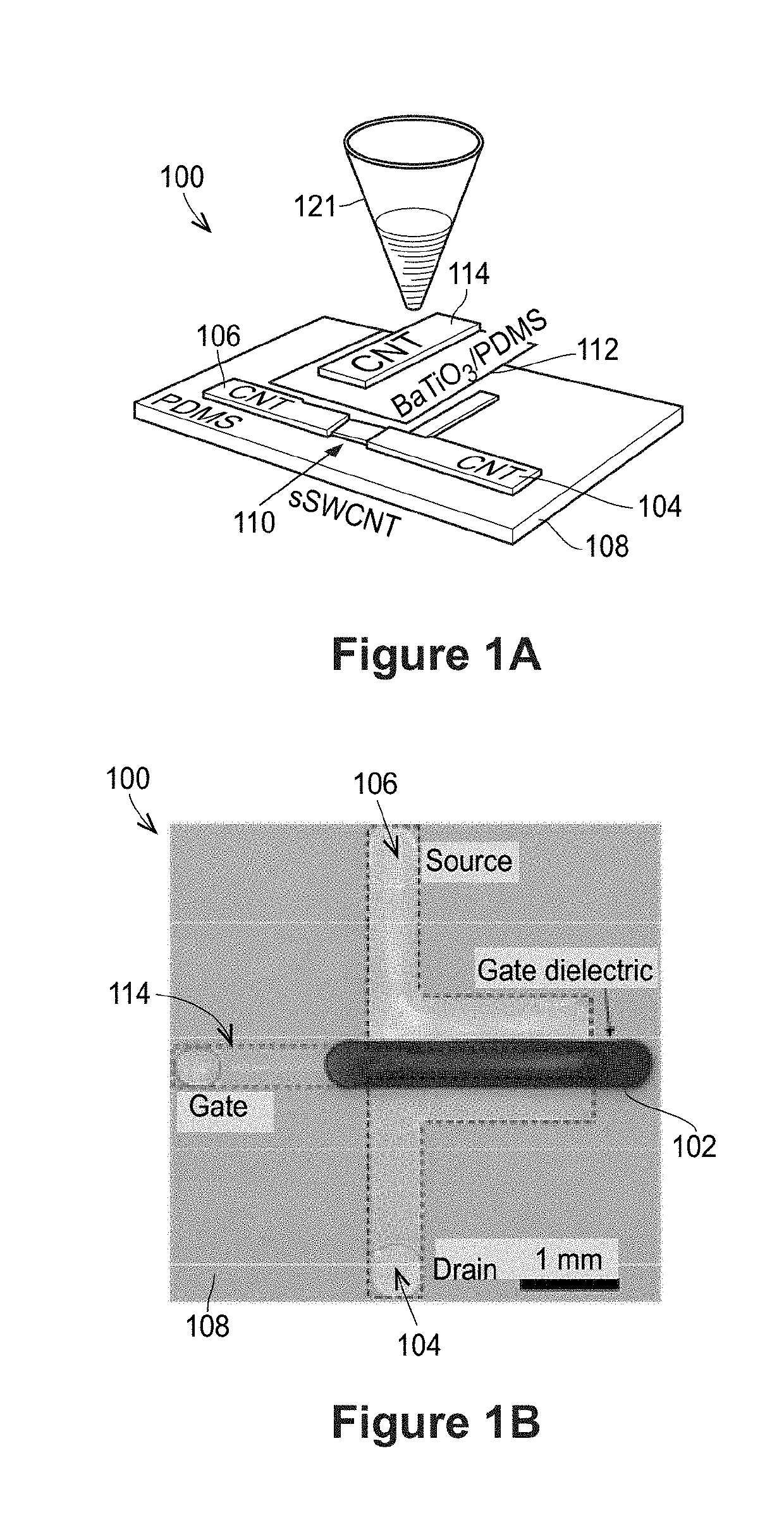
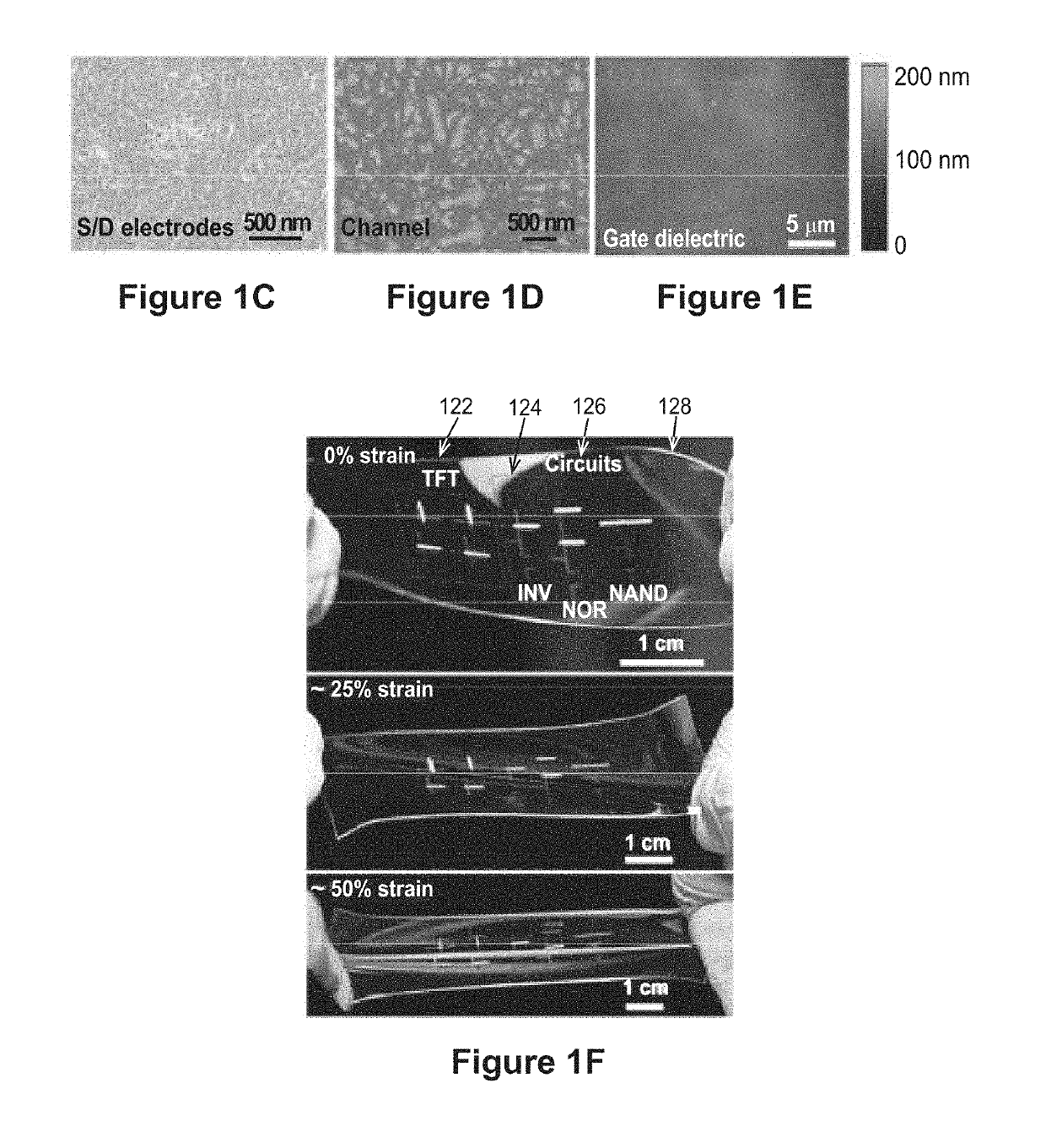
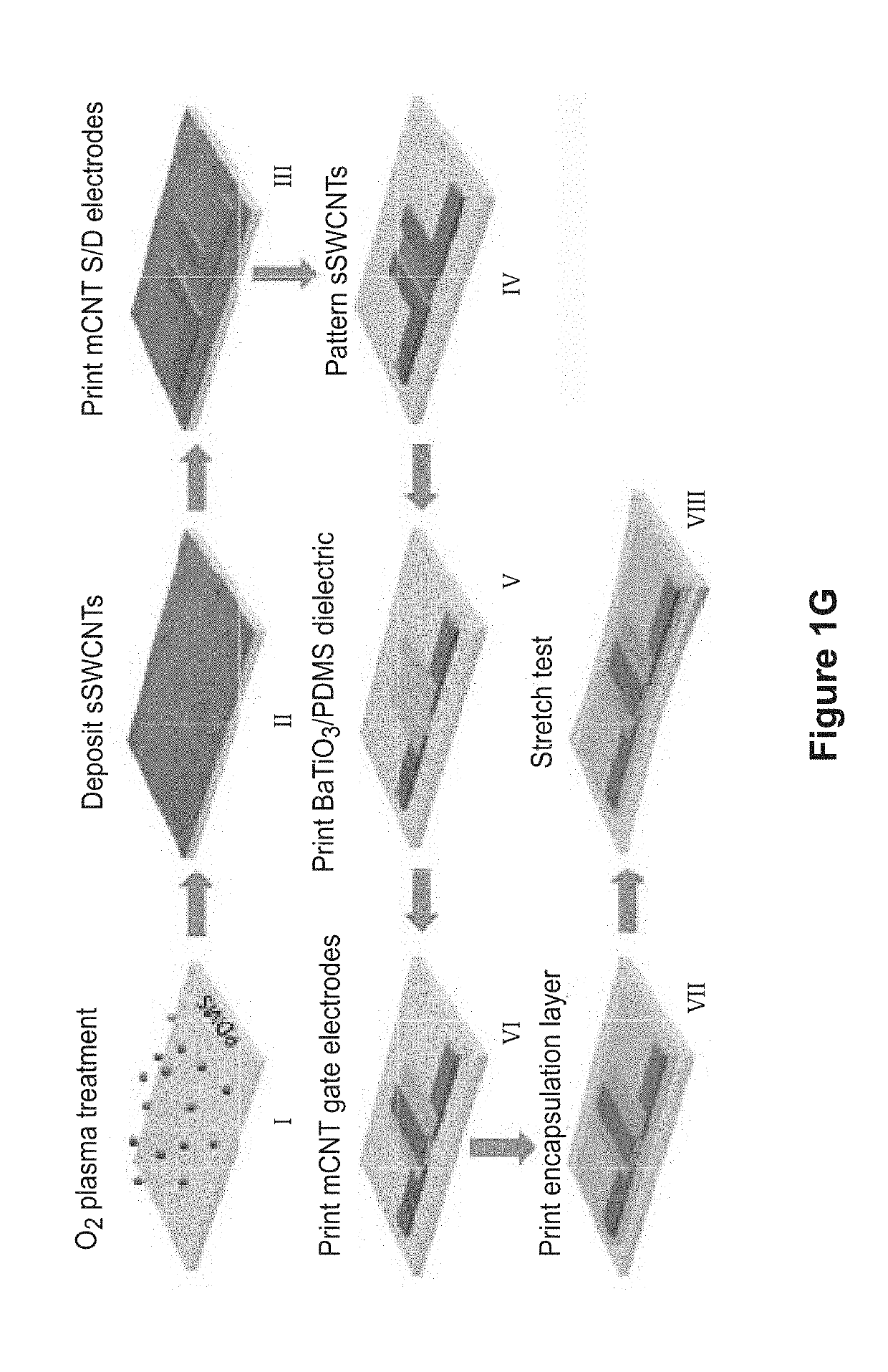
[0034]The present techniques provide intrinsically stretchable thin-film transistors (TFTs) and integrated logic circuits directly printed on elastomeric polydimethylsiloxane (PDMS) substrates. The printed devices utilize carbon nanotubes and a type of hybrid gate dielectric comprising PDMS and barium titanate (BaTiO3) nanoparticles. The BaTiO3 / PDMS composite simultaneously provides high dielectric constant, superior stretchability, low leakage, as well as good printability and compatibility with the elastomeric substrate. In example implementations, both TFTs and logic circuits may be stretched beyond 50% strain along either channel length or channel width directions for thousands of cycles while showing no significant degradation in electrical performance. The techniques may be implemented in sophisticated stretchable electronic systems with monolithically integrated sensors, actuators, and displays, fabricated by scalable and low-cost methods.

[0035]While various examples herein a...


PUM


Abstract

Printable and stretchable thin-film devices and fabrication techniques are provided for forming fully-printed, intrinsically stretchable thin-film transistors and integrated logic circuits using stretchable elastomer substrates such as polydimethylsiloxane (PDMS), semiconducting carbon nanotube network as channel, unsorted carbon nanotube network as source/drain/gate electrodes, and BaTiO3/PDMS composite as gate dielectric. Printable stretchable dielectric layer ink may be formed by mixing barium titanate nanoparticle (BaTiO3) with PDMS using 4-methyl-2-pentanone as solvent.

Description

CROSS-REFERENCE TO RELATED APPLICATIONS[0001]This application claims the benefit of U.S. Provisional Application Ser. No. 62 / 588,005, filed Nov. 17, 2017, entitled “Fully-Printed Stretchable Thin-Film Transistors And Integrated Logic Circuits” the entirety of which is hereby incorporated herein by reference.STATEMENT OF GOVERNMENT INTEREST[0002]This invention was made with support under ECCS1549888 awarded by the National Science Foundation. The government has certain rights in the invention.FIELD OF THE INVENTION[0003]The present disclosure relates generally to thin-film devices and, more particularly, to printable, intrinsically stretchable thin-film devices and fabrication techniques.BACKGROUND[0004]The background description provided herein is for the purpose of generally presenting the context of the disclosure. Work of the presently named inventors, to the extent it is described in this background section, as well as aspects of the description that may not otherwise qualify as...

Claims


Application Information

Patent Timeline
IPC IPC(8): H01L27/01H03K19/21H01L27/12H01L21/84H01L21/02
CPCH01L27/016H03K19/21H01L27/1214H01L21/84H01L21/02109H01L21/02118H01L21/02126H01L21/02288H01L21/3105Y02E10/549H10K85/221H10K10/84H01L29/4908H01L23/5387H01L29/517H10K77/111H10K10/478H10K10/481
Inventor WANG, CHUANCAI, LE
Owner BOARD OF TRUSTEES OPERATING MICHIGAN STATE UNIV
Why Eureka
Try Eureka