OLED package method and OLED package structure

a technology of oled and packaging, applied in the field of display technology, can solve the problems of low transmission rate, easy bending of fractures, and large stress of films, and achieve the effects of high heat conductivity and water and oxygen resistance, high transmission rate, and high bendability

Inactive Publication Date: 2019-05-23
WUHAN CHINA STAR OPTOELECTRONICS TECH CO LTD
View PDF2 Cites 1 Cited by
  • Summary
  • Abstract
  • Description
  • Claims
  • Application Information

AI Technical Summary

Benefits of technology

[0008]An objective of the present invention is to provide an OLED package method, which can promote the transmission rate, the bendable property, the high heat conductivity and the water and oxygen resistant property of the OLED thin film package layers, and thus to promote the usage performance and usage lifetime of the flexible OLED display panel.

Problems solved by technology

However, the density of the pure DLC film is higher, and thus, the transmission rate is not high and the stress of the film is very large, and the fracture can easily appears as being bent.

Method used


Image

  • OLED package method and OLED package structure
  • OLED package method and OLED package structure
  • OLED package method and OLED package structure

Examples


Embodiment Construction

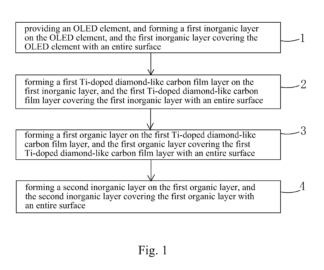
[0046]For better explaining the technical solution and the effect of the present invention, the present invention will be further described in detail with the accompanying drawings and the specific embodiments.

[0047]Please refer to FIG. 1, which is the first embodiment according to the OLED package method of the present invention, which comprises steps of:

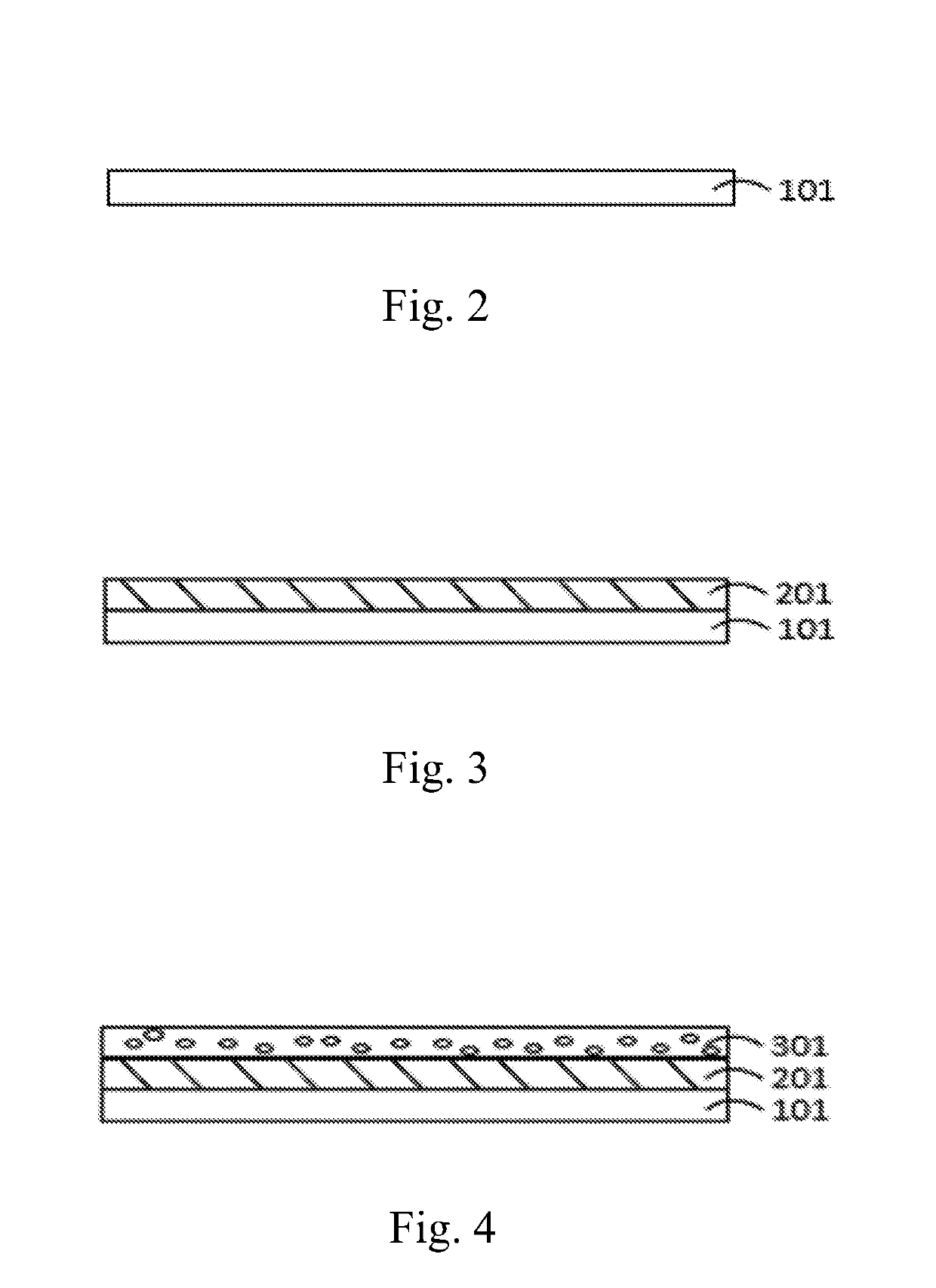
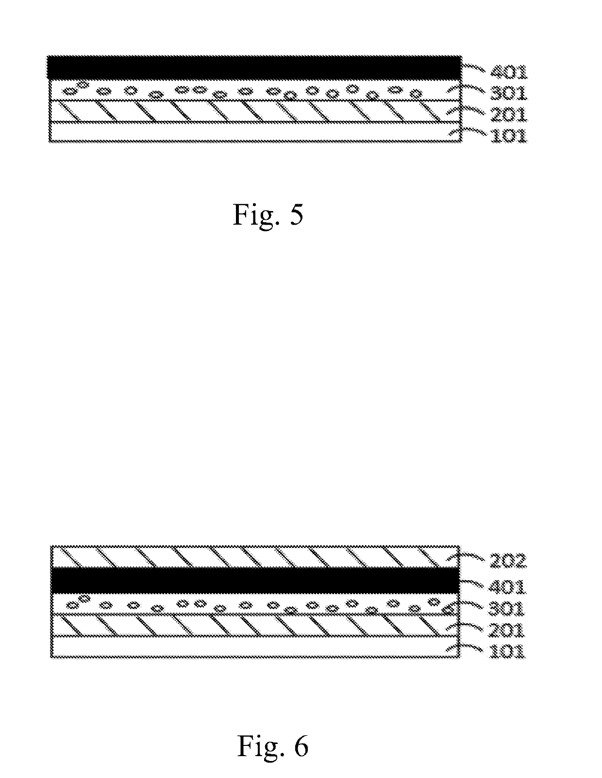
[0048]step 1, as shown in FIG. 2 and FIG. 3, providing an OLED element 101, and forming a first inorganic layer 201 on the OLED element 101, and the first inorganic layer 201 covering the OLED element 101 with an entire surface.

[0049]Specifically, in step 1, Plasma Enhanced Chemical Vapor Deposition (PECVD), Atomic Layer Deposition (ALD), Pulsed Laser Deposition (PLD) or Sputter is utilized to form the first inorganic layer 201.

[0050]Specifically, a material of the first inorganic layer 201 comprises one or more of aluminum oxide (Al2O3), titanium oxide (TiO2), silicon nitride (SiNx), silicon carbon nitride (SiCNx) and silicon oxid...


PUM

PropertyMeasurementUnit
luminescence efficiencyaaaaaaaaaa
densityaaaaaaaaaa
thermal conductivityaaaaaaaaaa

Abstract

The present invention provides an OLED package method and an OLED package structure. By introducing the Ti-doped diamond-like carbon film layer into the OLED thin film package layers and utilizing the higher transmission rate, the better flexibility, the high heat conductivity and lower water and oxygen permeation rate of the Ti-doped diamond-like carbon film layer, it can promote the transmission rate, the bendable property, the high heat conductivity and the water and oxygen resistant property of the OLED thin film package layers, and thus to promote the usage performance and usage lifetime of the flexible OLED display panel.

Description

FIELD OF THE INVENTION[0001]The present invention relates to a display technology field, and more particularly to an OLED package method and an OLED package structure.BACKGROUND OF THE INVENTION[0002]The Organic Light Emitting Display (OLED) device possesses many outstanding properties of self-illumination, low driving voltage, high luminescence efficiency, short response time, high clarity and contrast, near 180° view angle, wide range of working temperature, applicability of flexible display and large scale full color display. The OLED is considered as the most potential display device.[0003]The OLED can be categorized into two major types according to the driving ways, which are the Passive Matrix OLED (PMOLED) and the Active Matrix OLED (AMOLED), i.e. two types of the direct addressing and the Thin Film Transistor matrix addressing. The AMOLED comprises pixels arranged in array and belongs to active display type, which has high lighting efficiency and is generally utilized for t...

Claims


Application Information

Patent Timeline
Patent Type & Authority Applications(United States)
IPC IPC(8): H01L51/52H01L51/56C23C16/26
CPCH01L51/5256H01L51/56C23C16/26H01L2251/10H01L2251/5338H10K50/84H10K71/00H10K2102/302H10K50/8445H10K2102/311
Inventor PENG, SIMINJIN, JIANGJIANG
Owner WUHAN CHINA STAR OPTOELECTRONICS TECH CO LTD
Why Eureka
Try Eureka