Optical sensor and detector for an optical detection

a technology of optical detection and optical sensor, which is applied in the direction of radiation control devices, distance measurement, sustainable manufacturing/processing, etc., can solve the problems of requiring special attention for sub>2/sub>s in ald reactors, affecting the quality of optical detection, and affecting the detection effect, etc., to achieve the effect of easy integration and easy manufacturing

Active Publication Date: 2019-06-06
TRINAMIX GMBH
View PDF0 Cites 29 Cited by
  • Summary
  • Abstract
  • Description
  • Claims
  • Application Information

AI Technical Summary

Benefits of technology

[0023]More particular, it would be desirable to be capable of furnishing the optical sensor with an encapsulation layer that may especially be adapted to avoid degradation by external influence, such as by humidity and / or oxygen. Herein, it may be advantageous to use an encapsulation material which exhibits a suitable absorption characteristic and is, concurrently, easy to manufacture and easy to integrate on a circuit carrier device.

Problems solved by technology

The use of H2S in an ALD reactor requires special attention to safety issues due to its highly toxic, flammable, and corrosive nature.
Other encapsulation glasses, such as sapphire, may provide a more suitable absorption characteristic, but usually tend to be quite expensive.
In addition, hermetic packages generally turn out to be rather bulky, difficult to integrate on printed circuit boards, and expensive.
The low yields are apparently due to physical incompatibilities of the overcoating and the PbS film.

Method used


Image

  • Optical sensor and detector for an optical detection
  • Optical sensor and detector for an optical detection
  • Optical sensor and detector for an optical detection

Examples


Embodiment Construction

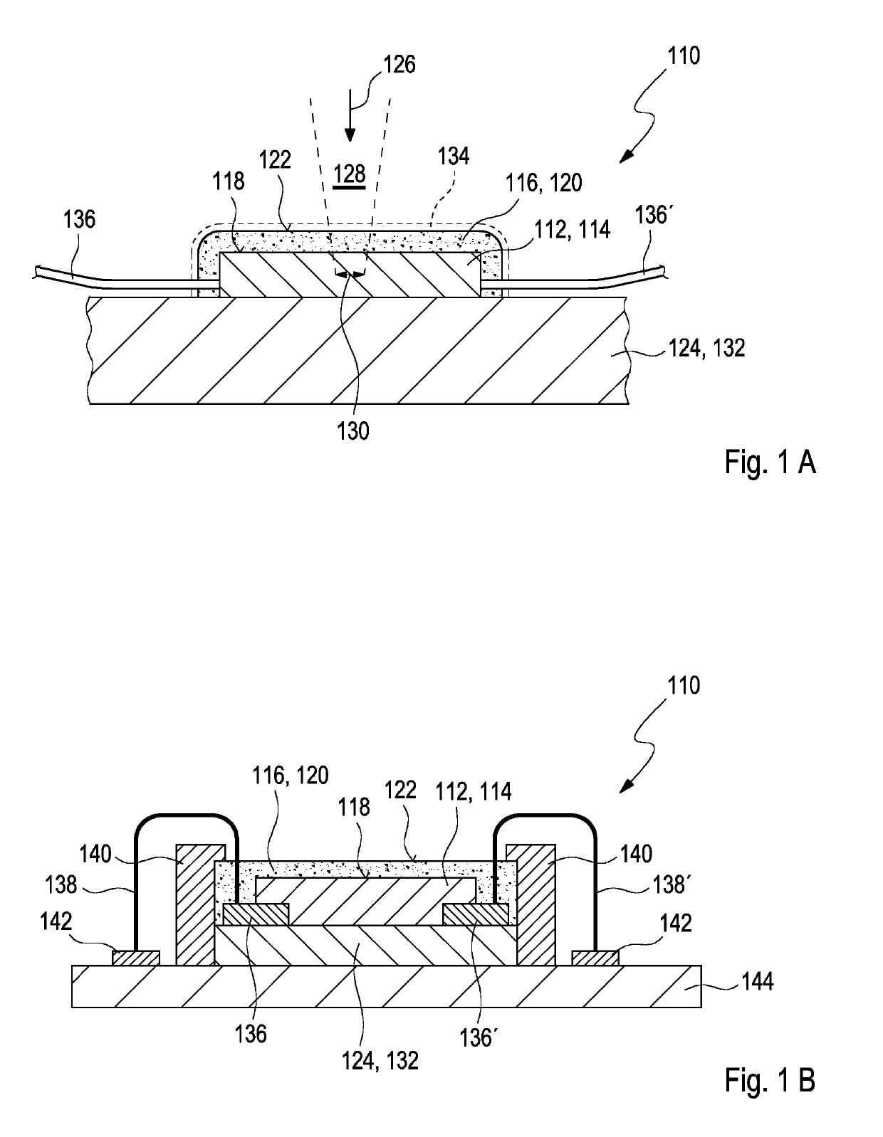
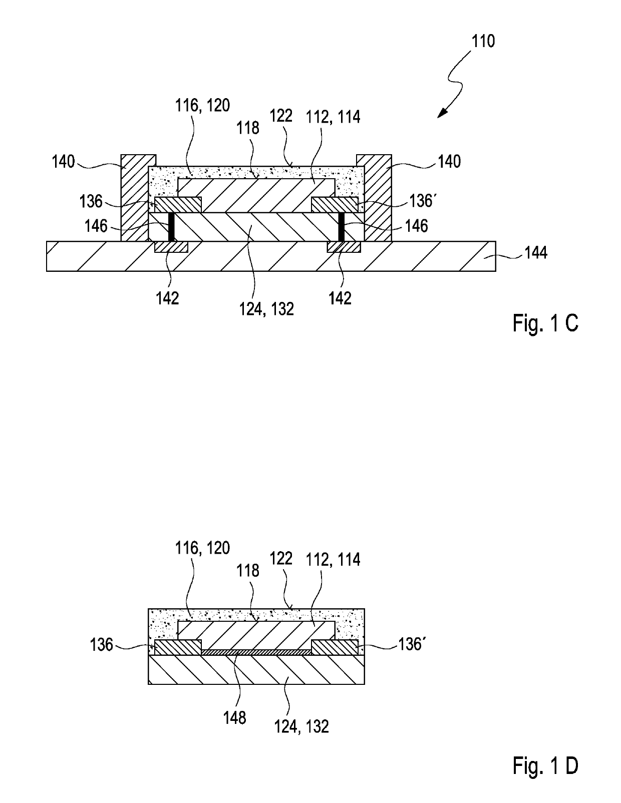
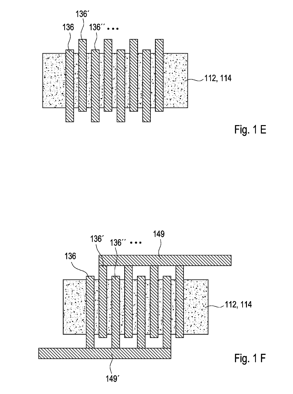
[0375]FIGS. 1A to 1F each illustrate, in a highly schematic fashion, an exemplary embodiment of an optical sensor 110 according to the present invention. Herein, FIGS. 1A to 1D present a side view of the optical sensor 110 while FIGS. 1E and 1F provide a top view only of a partition of the optical sensor 110. Further, FIG. 1G shows a transmission electron microscopy (TEM) image of the side view of a sample of the optical sensor 110 which has been prepared pursuant to the present invention.

[0376]Accordingly, the optical sensor 110 comprises a layer 112 of at least one photoconductive material 114. In particular, the layer 112 of the photoconductive material 114 may exhibit a thickness of 10 nm to 100 μm, preferably from 100 nm to 10 μm, in particular from 300 nm to 5 μm. In a preferred embodiment, the layer 112 of the photoconductive material 114 may comprise an essentially flat surface, wherein, however, other embodiments which may exhibit variations of the surface of the layer 112,...


PUM


Abstract

The present invention relates to an optical sensor, a detector comprising the optical sensor for an optical detection of at least one object, a method for manufacturing the optical sensor and various uses of the optical sensor and the detector. Furthermore, the invention relates to a human-machine interface, an entertainment device, a scanning system, a tracking system, a stereoscopic system, and a camera. The optical sensor (110) comprises a layer (112) of at least one photoconductive material (114), at least two individual electrical contacts (136, 136′) contacting the layer (112) of the photoconductive material (114), and a cover layer (116) deposited on the layer (112) of the photoconductive material (114), wherein the cover layer (116) is an amorphous layer comprising at least one metal-containing compound (120). The optical sensor (110) can be supplied as a non-bulkyhermetic package which, nevertheless, provides a high degree of protection against possible degradation by humidity and/or oxygen. Moreover, the cover layer (116) is capable of activating the photoconductive material (114) which results in an increased performance of the optical sensor (110). Further, the optical sensor (110) may be easily manufactured and integrated on a circuit carrier device.

Description

FIELD OF THE INVENTION[0001]The invention relates to an optical sensor and to a detector comprising such an optical sensor for an optical detection, in particular, of optical radiation, especially within the infrared spectral range, specifically with regard to sensing at least one of transmissivity, absorption, emission and reflectance, or of at least one object, especially, for determining a position of at least one object, specifically with regard to a depth or both to the depth and a width of the at least one object. Furthermore, the invention relates to a human-machine interface, an entertainment device, a scanning system, a tracking system, a stereoscopic system, and a camera. Further, the invention relates to a method for manufacturing the optical sensor and to various uses of the optical sensor and the detector. Such devices, methods and uses can be employed for example in various areas of daily life, gaming, traffic technology, mapping of spaces, production technology, secur...

Claims


Application Information

Patent Timeline
Patent Type & Authority Applications(United States)
IPC IPC(8): H01L31/09G01S17/48G01S7/481H01L27/146H01L31/02H01L31/0203H01L31/0216H01L31/0224H01L31/032H01L31/18
CPCH01L31/095G01S17/48G01S7/4816H01L27/14667H01L31/02016H01L31/0203H01L31/0216H01L31/0224H01L31/0324H01L31/1864H01L31/09H01L31/186G01S17/46H01L27/14665Y02E10/50Y02P70/50
Inventor HERMES, WILFRIEDVALOUCH, SEBASTIANSEND, ROBERTBRUDER, INGMARFEUERSTEIN, BERTRAM
Owner TRINAMIX GMBH
Why Eureka
Try Eureka