Microscale sensors for direct metrology of additively manufactured features

a technology of additive manufacturing and micro-scale sensors, which is applied in the direction of force measurement, instruments, and mechanical means, can solve the problems of not solving the specific problem of direct measurement of mechanical properties of submicron printed features in the past, and the commercial techniques for such direct measurements on the 100 nm feature scale are not available today, so as to improve the pattern transfer for the metallization step, simplify the fabrication process, and eliminate a number of post processing steps.

Active Publication Date: 2019-09-05
LAWRENCE LIVERMORE NAT SECURITY LLC +1
View PDF3 Cites 1 Cited by
  • Summary
  • Abstract
  • Description
  • Claims
  • Application Information

AI Technical Summary

Benefits of technology

[0062]One method for fabricating the MEMS sensors is through the PolyMUMPs approach. A silicon nitride layer, Nitride 1, is deposited to act as a hydrofluoric acid resistant electrical insulator. The base polysilicon layer, Poly 1, is deposited and patterned as the electrical traces for 37, 54a1, and 56a1 between the device fingers and the electrodes. Two sacrificial oxide layers, Oxide 1 and 2, create the gap, g, in FIG. 4, and open the holes for connections 54a and 56a between Poly 1 and the device layer, Poly 2. A thick polysilicon layer, Poly 2, is deposited, but not patterned to improve pattern transfer for the metallization step. Another nitride layer, Nitride 2, is deposited and patterned to open connections between Poly 2 and the Au/Cr metal electrode stack forming the

Problems solved by technology

However, this characterization for newly developed custom resists is often hindered by the lack of process knowledge required to successfully fabricate a mechanically stable macroscale part.
Unfortunately, commercial techniques for such direct measurements on the 100 nm feature scale are not available today.
The specific problem of direct measurement of the mechanical properties of submicron printed features has not been solved in the past.
This is not guaranteed for a newly synthesized custom resist.
In addition, all of these techniques generate structure-specific data that cannot be readily generalized beyond the specific structures tested.
The primary limitations of these devices for measurement of printed features are that (a) these sensors cannot be used to incorporate the printed features directly onto the sensors, and (b) pick-and-place techniques cannot

Method used


Image

  • Microscale sensors for direct metrology of additively manufactured features
  • Microscale sensors for direct metrology of additively manufactured features
  • Microscale sensors for direct metrology of additively manufactured features

Examples


Embodiment Construction

[0035]Example embodiments will now be described more fully with reference to the accompanying drawings.

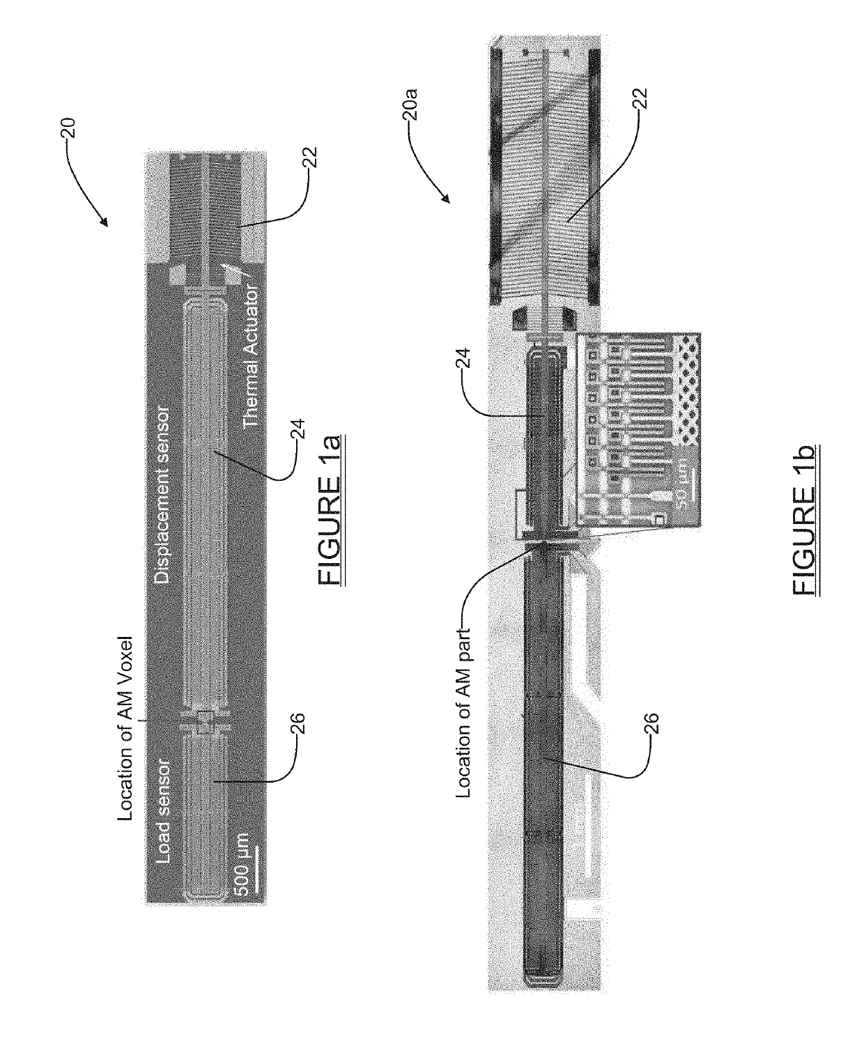
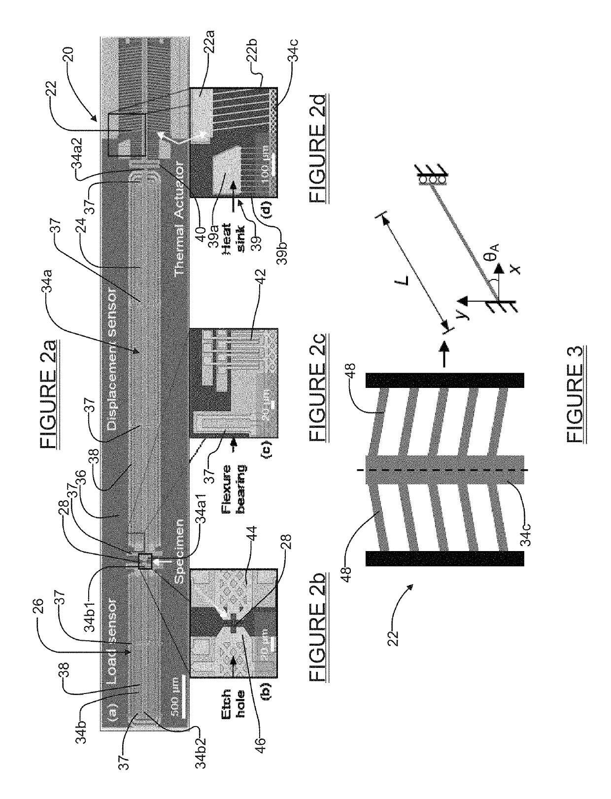
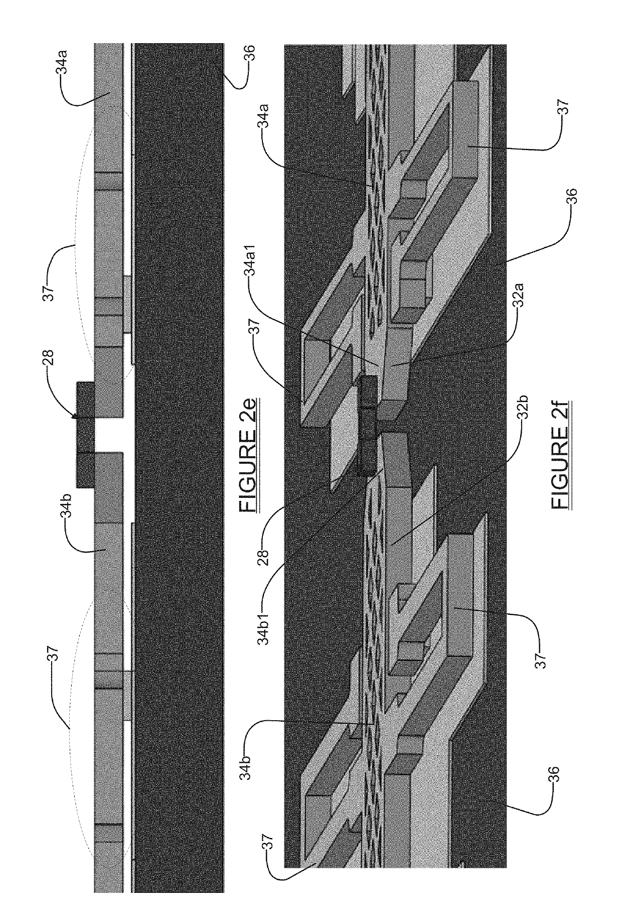
[0036]The system and method of the present disclosure enables direct measurement of the mechanical properties of submicron features on a scale that is relevant to additively manufacture larger structures. Specifically, the present disclosure enables measuring (a) stress-strain response of the elementary features, (b) strength of the elementary features and (c) strength and stiffness of a single stitch interface, i.e., the interface between two elementary features or between two assembled structures. The present disclosure overcomes the limitations of prior art systems and methods by enabling the printing of polymer features directly on top of the MEMS (Microelectromechanical System) sensors. To enable this integration, our devices have been designed to include features that suppress the stiction effect. This integration enables directly measuring the force-displacement response of ...


PUM


Abstract

This invention relates to a microelectromechanical device for mechanical characterization of a specimen. In one embodiment the device may incorporate a substrate, at least one first flexure bearing and at least one second flexure bearing, both being supported on the substrate. First and second movable shuttles may be used which are supported above the substrate by the flexure bearings so that each is free to move linearly relative to the substrate. Ends of the movable shuttles are separated by a gap. A thermal actuator may be connected to one end of the first movable shuttle, and operates to cause the first movable shuttle to move in a direction parallel to the surface of the substrate in response to a signal applied to the thermal actuator. A first capacitive sensor may be formed between the first movable shuttle and the substrate, and a second capacitive sensor formed between the second movable shuttle and the substrate.

Description

STATEMENT OF GOVERNMENT RIGHTS[0001]The United States Government has rights in this invention pursuant to Contract No. DE-AC52-07NA27344 between the U.S. Department of Energy and Lawrence Livermore National Security, LLC, for the operation of Lawrence Livermore National Laboratory.FIELD[0002]The present disclosure relates to systems and methods for performing metrology of polymeric additively manufactured structures comprising submicron features, and more particularly to systems and methods for directly measuring the stress-strain response of additively manufactured part or structure with a force and displacement resolution that is relevant to quantifying the stress-strain response of the individual submicron features comprising the additively manufactured part.BACKGROUND[0003]This section provides background information related to the present disclosure which is not necessarily prior art.[0004]Two-photon lithography is a popular technique to additively manufacture (“AM”) complex 3D...

Claims


Application Information

Patent Timeline
IPC IPC(8): G01N19/08G01B7/16B33Y40/00
CPCG01N19/08B33Y40/00G01B7/22G01N3/08G01N2203/0286G01L1/144G01L1/00B81C1/00
Inventor SAHA, SOURABHPANAS, ROBERTCULLINAN, MICHAEL A.LADNER, IAN SETH
Owner LAWRENCE LIVERMORE NAT SECURITY LLC
Why Eureka
Try Eureka