Electrophotographic photoconductor, method of manufacturing the same, and electrophotographic apparatus

a photoconductor and electrophotography technology, applied in the field of electrophotography, can solve the problems of shortening the lifetime of the photoconductor, changing the potential and the sensitivity, and image deficiencies, and achieves low residual potential, good wear resistance and contamination resistance, and high sensitivity.

Active Publication Date: 2019-11-14
FUJI ELECTRIC CO LTD
View PDF0 Cites 3 Cited by
  • Summary
  • Abstract
  • Description
  • Claims
  • Application Information

AI Technical Summary

Benefits of technology

[0025]According to the aspects described above, a photoconductor for electrophotography which has high sensitivity, low residual potential, and good wear resistance and contamination resistance, and is less likely to fall into light-induced fatigue and filming, and also has good potential stability throughout repeated printing even without a surface protective layer formed on a photosensitive layer, and a process of producing the photoconductor, and an electrophotographic apparatus can be provided.

Problems solved by technology

Furthermore, when paper dust or external additives remain on the blade, it may cause scratches on the surface of the organic photoconductor, shortening the lifetime of the photoconductor.
This may accelerate wearing of the photoconductor, which leads to changes in the potential and the sensitivity, causing image deficiencies.
This may cause deficiencies in the color balance and reproducibility in color electrophotographic apparatuses.
The presence of reverse polarity toner contained in a very small amount may lead to a problem that the toner cannot be sufficiently removed from the surface of the photoconductor and contaminates the charging device.
Furthermore, the surface of the photoconductor may be contaminated by ozone, nitrogen oxides and the like generated during charging of the photoconductor.
There are problems such as image deletion due to the contaminants themselves, as well as easy adhesion of paper dust and toner, blade squeaking and blade turn-over, and the susceptibility of the surface to scratches due to decreased lubricity of the surface of the photoconductor caused by adhered materials.
Unfortunately, in such a method including dispersing a filler in a film, it is difficult to uniformly disperse the filler.
Furthermore, the presence of filler aggregates, a reduction of transmission properties of the film, or scattering of the exposed light by the filler may cause problems that charge transport or charge generation ununiformly occurs, and that image characteristics are deteriorated.
However, since the dispersing material itself affects the characteristics of the photoconductor, it is difficult to obtain both good photoconductor characteristics and filler dispersibility.
However, the method described in Patent Document 4 has a problem that fluorine resins such as PTFE are poorly soluble in solvents or poorly compatible with other resins, which causes phase separation and light scattering at the interface between the resins.
For that reason, sensitivity characteristics required as a photoconductor cannot be achieved.
On the other hand, the method described in Patent Document 5 has a problem that the silicone resin bleeds into the coating surface, so that the effects cannot be obtained continuously.
Even such photoconductors have a problem with insufficient wear resistance depending on resins to be combined.
However, the methods of forming a surface protective layer have problems with difficulties of film formation on the charge transport layer and of sufficient achievement of both charge transport performance and charge retention function.
With regard to contamination resistance, there is a problem that, in the electrophotographic apparatus, the photoconductor is always in contact with a charging roller and a transfer roller, of which components exude to contaminate the surface of the photoconductor, leading to generation of black streaks in a halftone image.
However, these methods were not able to sufficiently meet the requirements for the contamination resistance.
Though having many advantages as photoconductor materials over inorganic materials as described above, organic materials obtained at present has not yet sufficiently achieved all of the characteristics required for photoconductors for electrophotography.
Thus, deterioration of the image quality is caused by the decrease of the charging potential, the increase of the residual potential, the change of the sensitivity and the like due to repeated use.

Method used


Image

  • Electrophotographic photoconductor, method of manufacturing the same, and electrophotographic apparatus
  • Electrophotographic photoconductor, method of manufacturing the same, and electrophotographic apparatus
  • Electrophotographic photoconductor, method of manufacturing the same, and electrophotographic apparatus

Examples


example 1

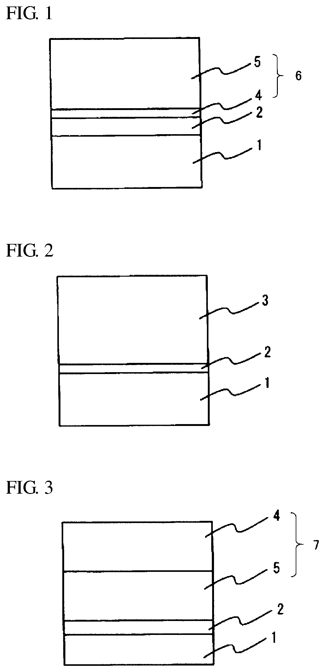
[0083]In 90 parts by mass of methanol, 5 parts by mass of alcohol-soluble nylon (Toray, product name “CM8000”) and 5 parts by mass of aminosilane-treated titanium oxide microparticles were dissolved and dispersed to prepare a coating liquid for undercoat layer. The coating liquid for undercoat layer was dip coated on the outer periphery of an aluminum cylinder with an outer diameter of 30 mm as a conductive substrate 1 and then dried at 100° C. for 30 minutes to form an undercoat layer 2 with a thickness of 3 μm.

[0084]In 60 parts by mass of dichloromethane, 1 part by mass of Y-titanyl phthalocyanine as a charge generation material and 1.5 parts by mass of polyvinyl butyral resin (Sekisui Chemical, product name “ESLEC KS-1”) as a binder resin were dissolved and dispersed to prepare a coating liquid for charge generation layer. The coating liquid for charge generation layer was dip coated on the undercoat layer 2 and then dried at 80° C. for 30 minutes to form a charge generation laye...

example 23

[0107]A coating liquid for forming an undercoat layer, which was prepared by dissolving 0.2 parts by mass of vinyl chloride-vinyl acetate-vinyl alcohol terpolymer (Nissin Chemical Industry, product name “Solbin TA5R”) in 99 parts by mass of methyl ethyl ketone while stirring, was dip coated on the outer periphery of an aluminum cylinder with an outer diameter of 24 mm as a conductive substrate 1 and then dried at 100° C. for 30 minutes to form an undercoat layer 2 with a thickness of 0.1μm.

[0108]Next, 1.5 parts by mass (about 1.2 parts by mass with respect to 100 parts by mass of a binder resin) of metal-free phthalocyanine as a charge generation material represented by the following formula:

45 parts by mass (about 34.6 parts by mass with respect to 100 parts by mass of a binder resin) of a compound represented by the above structural formula (1-5) as a hole transport material, 35 parts by mass (about 26.9 parts by mass with respect to 100 parts by mass of a binder resin) of a compo...

example 34

[0118]Next, 50 parts by mass of a compound as a hole transport material represented by the following formula:

and 50 parts by mass of bisphenol Z polycarbonate as a binder resin were dissolved in 800 parts by mass of dichloromethane to prepare a coating liquid for charge transport layer. The coating liquid for charge transport layer was dip coated on the outer periphery of an aluminum cylinder with an outer diameter of 24 mm as a conductive substrate 1 and then dried at 120° C. for 60 minutes to form a charge transport layer with a thickness of 15 μm.

[0119]Next, 1.5 parts by mass (about 2.5 parts by mass with respect to 100 parts by mass of a binder resin) of metal-free phthalocyanine as a charge generation material represented by the following formula:

10 parts by mass (about 17 parts by mass with respect to 100 parts by mass of a binder resin) of a compound represented by the above structural formula (1-5) as a hole transport material, 27.5 parts by mass (about 45.8 parts by mass wi...


PUM

PropertyMeasurementUnit
hole mobilityaaaaaaaaaa
diameteraaaaaaaaaa
thicknessaaaaaaaaaa

Abstract

Provided is a photoconductor for electrophotography having high sensitivity, low residual potential, and good wear resistance and contamination resistance, and that is less likely to cause light-induced fatigue and filming, and also exhibits good potential stability before and after repeated printing, even without a surface protective layer formed on a photosensitive layer. Provided also are a process of producing the photoconductor and an electrophotographic apparatus. The photoconductor for electrophotography includes a conductive substrate and a photosensitive layer formed on the conductive substrate and including a hole transport material having a structure represented by general formula (1) below; a binder resin having a repeating structure represented by general formula (2) below; and at least one electron transport material having a structure represented by general formulae (ET1) to (ET3) below:

Description

CROSS-REFERENCE TO RELATED APPLICATIONS[0001]This non-provisional application is a continuation of International Application No. PCT / JP2018 / 005599 filed on Feb. 16, 2018, the entire contents of which are incorporated herein by reference.BACKGROUND OF THE INVENTION1. Field of the Invention[0002]The present invention relates to a photoconductor for electrophotography (hereinafter also referred to as “photoconductor”), a process of producing the same, and an electrophotographic apparatus. More particularly, the present invention relates to a photoconductor for electrophotography mainly including a conductive substrate and a photosensitive layer containing an organic material and used in an electrophotographic printer, copier, fax machine and the like, a process of producing the same, and an electrophotographic apparatus.2. Background of the Related Art[0003]A photoconductor for electrophotography has a basic structure containing a photosensitive layer with a photoconductive function fo...

Claims


Application Information

Patent Timeline
Patent Type & Authority Applications(United States)
IPC IPC(8): G03G5/047G03G5/05G03G5/06
CPCG03G5/047G03G5/0525G03G5/0614G03G5/056G03G5/0564G03G5/0672G03G5/0616G03G5/0631G03G5/0609G03G5/0607G03G5/061473G03G5/04G03G5/0618
Inventor ZHU, FENGQIANGSUZUKI, SHINJIROKITAGAWA, SEIZO
Owner FUJI ELECTRIC CO LTD
Why Eureka
Try Eureka