Organic light-emitting element, and light-emitting material and fluorescent body used in same

a light-emitting element and light-emitting material technology, applied in the field of organic light-emitting devices, can solve the problems of low luminescent quantum efficiency of compounds, limited light emission efficiency improvement by fluorescence alone from the directly occurring excited singlet state, and cannot be expected to be applicable to the practical use of light-emitting device materials. , to achieve the effect of high light emission efficiency, delayed fluorescence, and high quantum yield

Active Publication Date: 2019-11-14
KYUSHU UNIV +1
View PDF0 Cites 2 Cited by
  • Summary
  • Abstract
  • Description
  • Claims
  • Application Information

AI Technical Summary

Benefits of technology

[0019]In the present invention, a compound capable of emitting delayed fluorescence and capable of undergoing intramolecular hydron transfer is used as a material of an organic light emitting device. The compound capable of emitting delayed fluorescence and capable of undergoing intramolecular hydron transfer exhibits a sufficiently high quantum yield enough for practical use even though not having a D-A type structure in a ground state thereof, and can be effectively used as a delayed fluorescent material for use in a light-emitting device. Consequently, the present invention can realize an organic light-emitting device having a high light emission efficiency and can realize a delayed fluorescent material having a broad latitude in molecular planning of a delayed fluorescent material, having high planarity and having good stability or alignability.

Problems solved by technology

For example, in current excitation of a compound, the occurring probability of the excited singlet state to the excited triplet state is 25% / 75%, and therefore improvement of light emission efficiency by the fluorescence alone from the directly occurring excited singlet state is limited.
All these compounds have a low luminescent quantum efficiency, and therefore could not be expected to be applicable to practical use for light-emitting device materials.

Method used


Image

  • Organic light-emitting element, and light-emitting material and fluorescent body used in same
  • Organic light-emitting element, and light-emitting material and fluorescent body used in same
  • Organic light-emitting element, and light-emitting material and fluorescent body used in same

Examples


example 1

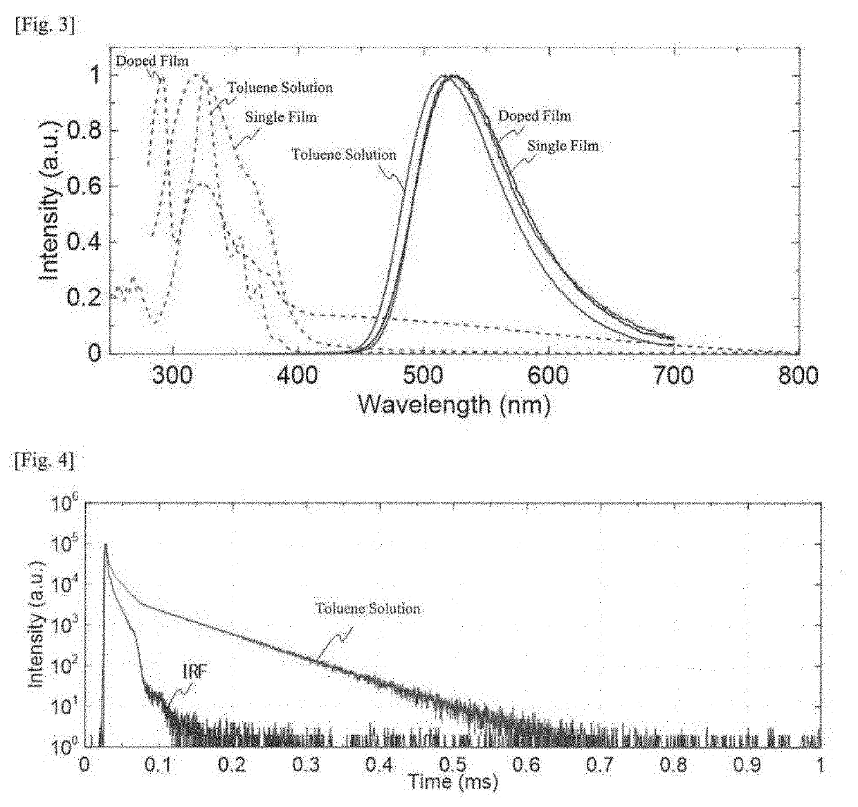
[0119]The compound 1 was dissolved in dimethylformamide, tetrahydrofuran or toluene to prepare solutions thereof (concentration 10−5 mol / L).

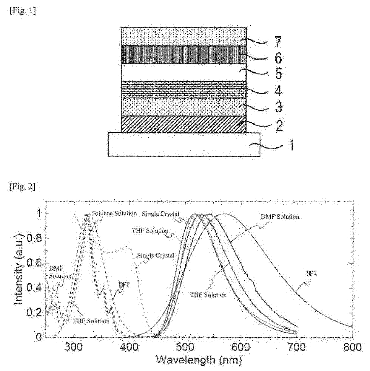
[0120]According to a sublimation method, a single crystal of the compound 1 was formed to be an organic photoluminescent device. In X-ray structural analysis, all the atoms of the resultant crystal were in one and the same plane, RMS (root-mean-square) of the other atoms than 1H was 0.036 angstroms, and the compound had high planarity.

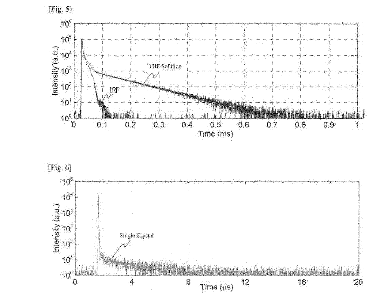
[0121]According to a vacuum evaporation method, a thin film of the compound 1 (hereinafter referred to as “single film”) was formed on a quartz substrate under the condition of a vacuum degree of 10−3 Pa or less, in a thickness of 50 to 100 nm to be an organic photoluminescent device.

[0122]Apart from this and according to a vacuum evaporation method, the compound 1 and DPEPO were vapor-deposited from different evaporation sources on a quartz substrate under the condition of a vacuum degree of 10−3 Pa or less to for...

example 2

[0138]On a glass substrate with an anode of indium tin oxide (ITO) having a thickness of 100 nm formed thereon, thin films were layered according to a vacuum vapor deposition method under a vacuum degree of 10−4 Pa. First, on ITO, TAPC was formed in a thickness of 30 nm. Subsequently, TCTA was formed thereon in a thickness of 20 nm, and further on this, CzSi was formed in a thickness of 10 nm. Next, the compound 1 and PPT were co-deposited from different evaporation sources to form a layer having a thickness of 30 nm as a light-emitting layer. At this time, the concentration of the compound 1 was 10% by weight. Next, PPT was formed in a thickness of 40 nm. Further, lithium fluoride (LiF) was vapor-deposited in a thickness of 0.8 nm, and then aluminum (Al) was vapor-deposited thereon in a thickness of 100 nm to form a cathode, thereby producing an organic electroluminescent device.

[0139]FIG. 16 shows light emission spectra of the produced organic electroluminescent device measured at...

example 3

[0140]An organic electroluminescent device was produced in the same manner as in Example 2, except that NPD was formed in a thickness of 30 nm on ITO in place of forming TAPC in a thickness of 30 nm thereon.

[0141]FIG. 19 shows light emission spectra of the produced organic electroluminescent device measured at a voltage of 6 V, 9 V and 12 V; FIG. 20 shows a current density-voltage characteristic thereof; and FIG. 21 shows an external quantum efficiency (EQE)-current density characteristic thereof. The organic electroluminescent device using the compound 1 as a light-emitting material attained a high external quantum efficiency of 9.4%.


PUM

PropertyMeasurementUnit
triplet energy levelaaaaaaaaaa
energy levelaaaaaaaaaa
temperatureaaaaaaaaaa

Abstract

Disclosed is an organic light-emitting device using a compound capable of emitting delayed fluorescence and capable of undergoing intramolecular hydron transfer. The compound includes, for example, a compound represented by the general formula. X1 to X3 each represent O or S; R1 to R6 each represent nH or a substituent; n, n1 to n3 each represent an integer of 1 to 3.

Description

TECHNICAL FIELD[0001]The present invention relates to an organic light-emitting device using a compound that emits delayed fluorescence.BACKGROUND ART[0002]Studies for enhancing the light emission efficiency of organic light-emitting devices such as organic electroluminescent devices (organic EL devices) are being made actively. In particular, various kinds of efforts have been made for increasing light emission efficiency by newly developing and combining an electron transfer material, a hole transfer material, a light-emitting material and others to constitute an organic electroluminescent device. Among them, there is known a study relating to an organic electroluminescent device that utilizes a thermal activation type delayed fluorescent material.[0003]A thermal activation type delayed fluorescent material is a compound which, after having transited to an excited triplet state, undergoes reverse intersystem crossing from the excited triplet state to an excited singlet state throu...

Claims


Application Information

Patent Timeline
Patent Type & Authority Applications(United States)
IPC IPC(8): H01L51/00H01L51/50C09K11/06
CPCH01L51/0072C09K2211/1011H01L51/5016H01L51/5004C09K11/06C07D471/14H10K85/6572H10K85/324H10K50/11H10K2101/20H10K2101/10H10K2101/40
Inventor MAMADA, MASASHIADACHI, CHIHAYANAKANOTANI, HAJIMEYANG, YUSEOK
Owner KYUSHU UNIV
Why Eureka
Try Eureka